ZHCSBK4G March   2013  – March 2019

PRODUCTION DATA.  

  1. 特性
  2. 应用
  3. 说明
    1.     Device Images
      1.      典型应用原理图
      2.      充电器效率与输入电压
  4. 修订历史记录
  5. Pin Configuration and Functions
    1.     Pin Functions
  6. Specifications
    1. 6.1 Absolute Maximum Ratings
    2. 6.2 ESD Ratings
    3. 6.3 Recommended Operating Conditions
    4. 6.4 Thermal Information
    5. 6.5 Electrical Characteristics
    6. 6.6 Electrical Characteristics
    7. 6.7 Typical Characteristics
  7. Detailed Description
    1. 7.1 Overview
    2. 7.2 Functional Block Diagram
    3. 7.3 Feature Description
      1. 7.3.1 Maximum Power Point Tracking
      2. 7.3.2 Battery Undervoltage Protection
      3. 7.3.3 Battery Overvoltage Protection
      4. 7.3.4 Battery Voltage within Operating Range (VBAT_OK Output)
      5. 7.3.5 Storage Element / Battery Management
      6. 7.3.6 Programming OUT Regulation Voltage
      7. 7.3.7 Step Down (Buck) Converter
      8. 7.3.8 Nano-Power Management and Efficiency
    4. 7.4 Device Functional Modes
      1. 7.4.1 Main Boost Charger Disabled (Ship Mode) - (VSTOR > VSTOR_CHGEN and EN = HIGH)
      2. 7.4.2 Cold-Start Operation (VSTOR < VSTOR_CHGEN, VIN_DC > VIN(CS) and PIN > PIN(CS), EN = don't care)
      3. 7.4.3 Main Boost Charger Enabled (VSTOR > VSTOR_CHGEN and EN = LOW )
        1. 7.4.3.1 Buck Converter Enabled (VSTOR > VBAT_UV, EN = LOW and VOUT_EN = HIGH )
      4. 7.4.4 Thermal Shutdown
  8. Application and Implementation
    1. 8.1 Application Information
      1. 8.1.1 Energy Harvester Selection
      2. 8.1.2 Storage Element Selection
      3. 8.1.3 Inductor Selection
        1. 8.1.3.1 Boost Charger Inductor Selection
        2. 8.1.3.2 Buck Converter Inductor Selection
      4. 8.1.4 Capacitor Selection
        1. 8.1.4.1 VREF_SAMP Capacitance
        2. 8.1.4.2 VIN_DC Capacitance
        3. 8.1.4.3 VSTOR Capacitance
        4. 8.1.4.4 VOUT Capacitance
        5. 8.1.4.5 Additional Capacitance on VSTOR or VBAT
    2. 8.2 Typical Applications
      1. 8.2.1 Solar Application Circuit
        1. 8.2.1.1 Design Requirements
        2. 8.2.1.2 Detailed Design Procedure
        3. 8.2.1.3 Application Curves
      2. 8.2.2 TEG Application Circuit
        1. 8.2.2.1 Design Requirements
        2. 8.2.2.2 Detailed Design Procedure
        3. 8.2.2.3 Application Curves
      3. 8.2.3 Piezoelectric Application Circuit
        1. 8.2.3.1 Design Requirements
        2. 8.2.3.2 Detailed Design Procedure
        3. 8.2.3.3 Application Curves
  9. Power Supply Recommendations
  10. 10Layout
    1. 10.1 Layout Guidelines
    2. 10.2 Layout Example
    3. 10.3 Thermal Considerations
  11. 11器件和文档支持
    1. 11.1 器件支持
      1. 11.1.1 第三方米6体育平台手机版_好二三四免责声明
    2. 11.2 文档支持
      1. 11.2.1 相关文档
    3. 11.3 接收文档更新通知
    4. 11.4 社区资源
    5. 11.5 商标
    6. 11.6 静电放电警告
    7. 11.7 术语表
  12. 12机械、封装和可订购信息

封装选项

机械数据 (封装 | 引脚)
散热焊盘机械数据 (封装 | 引脚)
订购信息

Application Curves

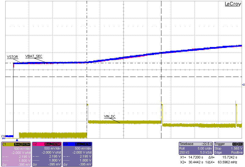
bq25570 app3_startup_1VIN_8p5ma_100kohm_slusbj3.png
Sourcemeter with VSOURCE = 1.0 V and compliance of 8.5 mA subsequently applied to VIN_DC
VBAT = 0.1 F capacitor charged to 2.2 V
Resistance on VSTOR = 100 kΩ
Figure 43. Startup by Battery Attach With Partially Charged Storage Element
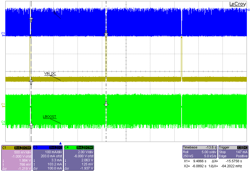
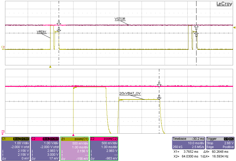
bq25570 app3_mppt_ov_3p3v_3vstor_2p0vin_42p6ma_slusbj3.png
VIN_DC = sourcemeter with VSOURCE = 2.0 V and compliance
of 43 mA
VBAT = sourcemeter with VSOURCE = 3.0 V and compliance
of 1 A
Figure 45. MPPT Operation
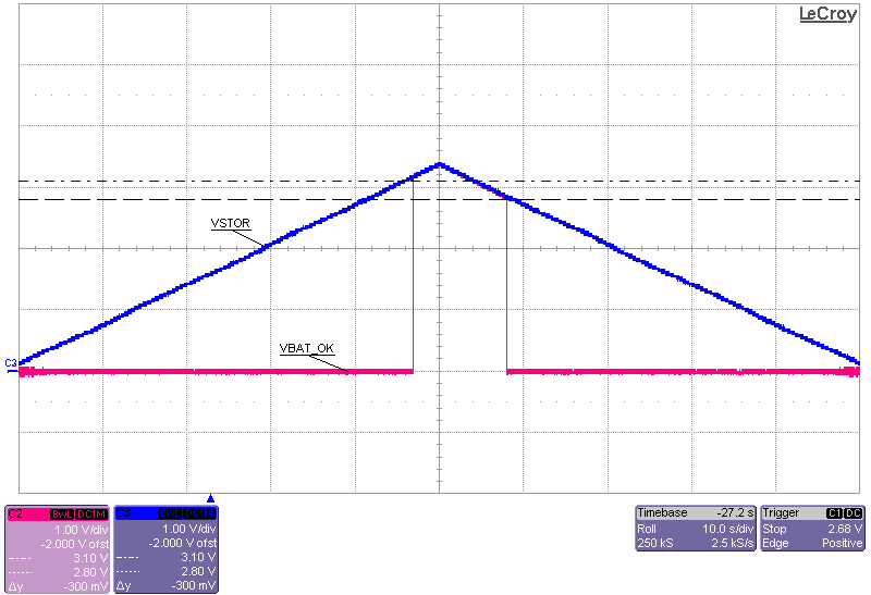
bq25570 app3_ov_3p3v_Vbatok_slusbj3.png
VIN_DC floating
No storage element on VBAT or VBAT_PRI
VSTOR artifically ramped from 0 V to 3.3 V to 0 V using a function generator
Figure 47. VBAT_OK Operation
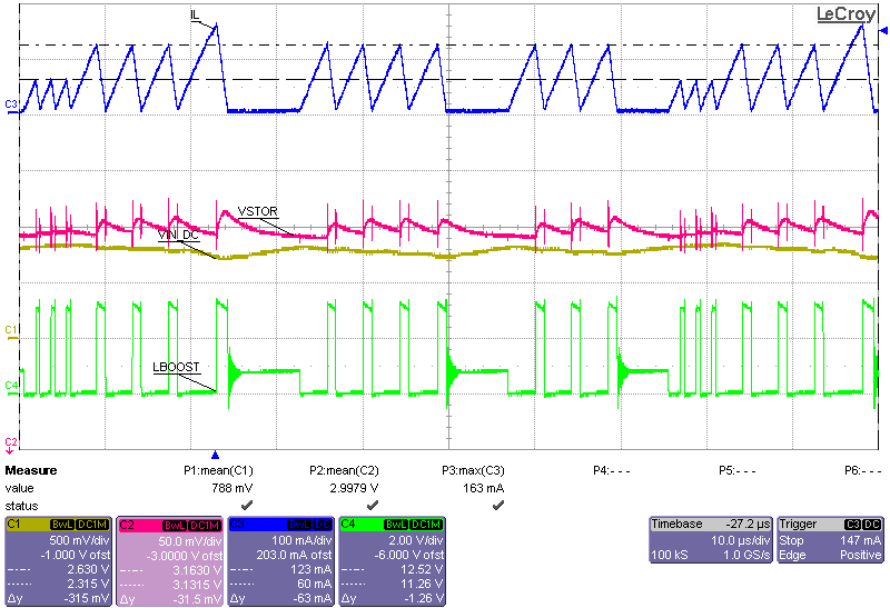
bq25570 app3_operation_ov_3p3v_3vstor_2p0vin_42p6ma_slusbj3.png
VIN_DC = sourcemeter with VSOURCE = 2.0 V and compliance of 43 mA
VBAT = sourcemeter with VSOURCE = 3.0 V and compliance of
1 A
Figure 44. Boost Charger Operational Waveforms
bq25570 app3_ov_3p3v_VRDIV_slusbj3.png
VIN_DC = sourcemeter with VSOURCE = 2.0 V and compliance of 43 mA
VBAT = sourcemeter with VSOURCE = 3.0 V and compliance of 1 A
Figure 46. VRDIV Waveform