ZHCSLT1B december 2020 – july 2023 BQ25672
PRODUCTION DATA
- 1
- 1 特性
- 2 应用
- 3 说明
- 4 Revision History
- 5 说明(续)
- 6 Pin Configuration and Functions
- 7 Specifications
-
8 Detailed Description
- 8.1 Overview
- 8.2 Functional Block Diagram
- 8.3
Feature Description
- 8.3.1 Device Power-On-Reset
- 8.3.2 PROG Pin Configuration
- 8.3.3 Device Power Up from Battery without Input Source
- 8.3.4 Device Power Up from Input Source
- 8.3.5 Dual-Input Power Mux
- 8.3.6 Buck Converter Operation
- 8.3.7 USB On-The-Go (OTG)
- 8.3.8 Power Path Management
- 8.3.9 Battery Charging Management
- 8.3.10 Integrated 16-Bit ADC for Monitoring
- 8.3.11 Status Outputs ( STAT, and INT)
- 8.3.12 Ship FET Control
- 8.3.13
Protections
- 8.3.13.1
Voltage and Current Monitoring
- 8.3.13.1.1 VAC Over-voltage Protection (VAC_OVP)
- 8.3.13.1.2 VBUS Over-voltage Protection (VBUS_OVP)
- 8.3.13.1.3 VBUS Under-voltage Protection (POORSRC)
- 8.3.13.1.4 System Over-voltage Protection (VSYS_OVP)
- 8.3.13.1.5 System Short Protection (VSYS_SHORT)
- 8.3.13.1.6 Battery Over-voltage Protection (VBAT_OVP)
- 8.3.13.1.7 Battery Over-current Protection (IBAT_OCP)
- 8.3.13.1.8 Input Over-current Protection (IBUS_OCP)
- 8.3.13.1.9 OTG Over-voltage Protection (OTG_OVP)
- 8.3.13.1.10 OTG Under-voltage Protection (OTG_UVP)
- 8.3.13.2 Thermal Regulation and Thermal Shutdown
- 8.3.13.1
Voltage and Current Monitoring
- 8.3.14 Serial Interface
- 8.4 Device Functional Modes
- 8.5 Register Map
- 9 Application and Implementation
- 10Power Supply Recommendations
- 11Layout
- 12Device and Documentation Support
- 13Mechanical, Packaging, and Orderable Information
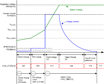
8.3.9.2 Battery Charging Profile
The device charges the battery in five phases: trickle charge, pre-charge, constant current, constant voltage, and top-off trickle charging (optional). At the beginning of a charging cycle, the device checks the battery voltage and regulates current/voltage accordingly.
| VBAT | CHARGING CURRENT | REGISTER DEFAULT SETTING | CHRG_STAT |
|---|---|---|---|
| < VBAT_SHORT | IBAT_SHORT | 100 mA | 001 |
| VBAT_SHORTZ to VBAT_LOWV | IPRECHG | 120 mA | 010 |
| > VBAT_LOWV | ICHG | 1 A | 011 |
If the charger is in DPM regulation or thermal regulation during charging, the actual charging current is less than the programmed value. In this case, termination is temporarily disabled and the charging safety timer is counted at half the clock rate, as explained in Charging Safety Timer.
The VBAT_SHORTZ is the battery voltage threshold for the transition from trickle charge to pre-charge, which is fixed value 2.2V. During the trickle charge to pre-charge transition, the charger regulates the battery voltage to 2.5V/cell typical for tBAT_SHORTZ duration. VBAT_LOWV is the battery voltage threshold for the transition from pre-charge to fast charge. It is defined as a ratio of battery voltage regulation limit (VREG).
During SYSMIN regulation with BATFET LDO operation, the charge current is limited to 2 A maximum, regardless of the charge current register setting being set higher than 2 A, in order to protect the BATFET. The BATFET LDO operation can be disabled by setting DIS_LDO = 1. In this condition, the pre-charge current and fast charge current are both regulated by the buck converter PWM current regulation loop. The SYS is no longer regulated to VSYSMIN when the LDO mode is disabled at the low battery voltage condition. When in trickle charge, setting DIS_LDO = 1 does not affect IBAT_SHORT or VSYSMIN operation.
 Figure 8-10 Battery Charging Profile