ZHCSLT1B december 2020 – july 2023 BQ25672
PRODUCTION DATA
- 1
- 1 特性
- 2 应用
- 3 说明
- 4 Revision History
- 5 说明(续)
- 6 Pin Configuration and Functions
- 7 Specifications
-
8 Detailed Description
- 8.1 Overview
- 8.2 Functional Block Diagram
- 8.3
Feature Description
- 8.3.1 Device Power-On-Reset
- 8.3.2 PROG Pin Configuration
- 8.3.3 Device Power Up from Battery without Input Source
- 8.3.4 Device Power Up from Input Source
- 8.3.5 Dual-Input Power Mux
- 8.3.6 Buck Converter Operation
- 8.3.7 USB On-The-Go (OTG)
- 8.3.8 Power Path Management
- 8.3.9 Battery Charging Management
- 8.3.10 Integrated 16-Bit ADC for Monitoring
- 8.3.11 Status Outputs ( STAT, and INT)
- 8.3.12 Ship FET Control
- 8.3.13
Protections
- 8.3.13.1
Voltage and Current Monitoring
- 8.3.13.1.1 VAC Over-voltage Protection (VAC_OVP)
- 8.3.13.1.2 VBUS Over-voltage Protection (VBUS_OVP)
- 8.3.13.1.3 VBUS Under-voltage Protection (POORSRC)
- 8.3.13.1.4 System Over-voltage Protection (VSYS_OVP)
- 8.3.13.1.5 System Short Protection (VSYS_SHORT)
- 8.3.13.1.6 Battery Over-voltage Protection (VBAT_OVP)
- 8.3.13.1.7 Battery Over-current Protection (IBAT_OCP)
- 8.3.13.1.8 Input Over-current Protection (IBUS_OCP)
- 8.3.13.1.9 OTG Over-voltage Protection (OTG_OVP)
- 8.3.13.1.10 OTG Under-voltage Protection (OTG_UVP)
- 8.3.13.2 Thermal Regulation and Thermal Shutdown
- 8.3.13.1
Voltage and Current Monitoring
- 8.3.14 Serial Interface
- 8.4 Device Functional Modes
- 8.5 Register Map
- 9 Application and Implementation
- 10Power Supply Recommendations
- 11Layout
- 12Device and Documentation Support
- 13Mechanical, Packaging, and Orderable Information
8.3.5.3 Two ACFETs-RBFETs
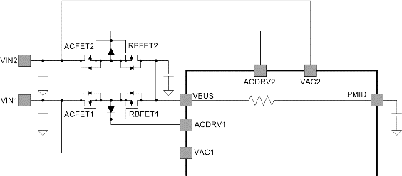
In this scenario, both ACFET1-RBFET1 and ACFET2-RBFET2 are present. VAC1 / VAC2 is tied to the drain of ACFET1 / ACFET2, ACDRV1 / ACDRV2 is connected to the gate of ACFET1 / ACFET2. This structure is developed to support dual-input connected at VA1 and VAC2.
 Figure 8-4 Two ACFETs-RBFETs Structure Supporting One Input at VAC1 and One Input at VAC2
- At POR, the charger detects both ACFET1-RBFET1 and ACFET2-RBFET2 presented, then updates ACRB1_STAT and ACRB2_STAT to 1.
- EN_ACDRV1 and EN_ACDRV2 are programmable in this case.
- The ACDRV turns on the ACFET-RBFET of the port with a valid input presented first. The other ACFET-RBFET stays off, even if there is an adapter being plugged in later.
- Programming EN_ACDRV1 = 1, EN_ACDRV2 = 1 at the same time to turn on both ACFET1-RBFET1 and ACFET2-RBFET2 is not allowed, which will be ignored by the charger.
- Assuming two valid voltages are presented at VAC1 and VAC2, ACFET1-RBFET1 turns on, connecting the input source at VAC1 to VBUS. If the voltage at VAC1 becomes invalid because of VAC_UVLO, VAC_OV or IBUS_OC, the charger swaps the input from VAC1 to VAC2, by turning off ACFET1-RBFET1 and then turning on ACFET2-RBFET2, without any host engagement. Swapping the input from VAC1 to VAC2 also can be controlled by the host. For example, to swap VAC1 to VAC2, the host can program REG0x13[7:6] (EN_ACDRV2, EN_ACDRV1) from 01b to 10b. The same control logic is applied to the input swapping from VAC2 to VAC1.
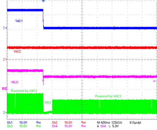
The waveforms below show the charger input transition from VAC1 to VAC2 when VAC1 is disconnected. At the beginning, VAC1 = 12V and VAC2 = 8V are both present. When VAC1 = 12V is gone, the charger accomplishes the input source auto transition from VAC1 to VAC2 without host control.
 Figure 8-5 Input Source Auto Transition from VAC1 to VAC2 when VAC1 is Gone
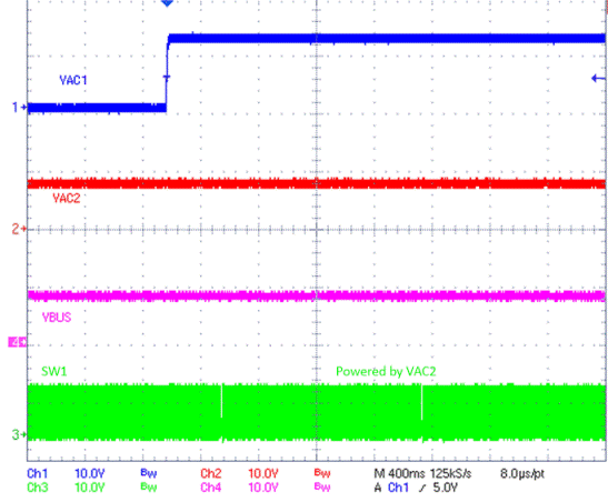
When VAC2 has been connected, even if VAC1 is re-plugged in again later, the charger still stays connecting VAC2 as the input source, which is illustrated as the waveforms below. The host has to be involved to swap the input source from VAC2 back to VAC1 if necessary.
 Figure 8-6 VAC1 Re-Plugged in When VAC2 Connected as the Charger Input
Some other critical notes for the application of this dual input power MUX are list below:
- The register bits, EN_ACDRV1 and EN_ACDRV2, are not only to control the turning on / off of ACFETs-RBFETs but also to indicate the on / off status of the FETs.
- The charger also provides the fault protection by turning ACFETs-RBFETs off, such as VAC_OVP and IBUS_OCP.
- With only one valid input presented at either VAC1 or VAC2, the ACFET1-RBFET1 and ACFET2-RBFET2 can not be both turned off by setting REG0x13[7:6] = 00b, because the charger is always trying to connect the only one input voltage available to power the charger. At this condition, the host has to set DIS_ACDRV = 1 to force both two ACFETs-RBFETs off. With two input sources presented at both VAC1 and VAC2, the host can turn of the two ACFETs-RBFETs by setting either REG0x13[7:6] = 00 or DIS_ACDRV = 1.
- In the transition from one input to the other one, after one ACFET-RBFET is turned off, the other one turns on until the VBUS voltage drops lower than VBUS_PRESENT. The converter stops switching for a short time period. When no battery presented or battery depleted, the system output would fall. The user has to be aware of this and avoid the input source swap when the battery voltage is too low.