SLUSCU2 November 2017
PRODUCTION DATA.
- 1 Features
- 2 Applications
- 3 Description
- 4 Revision History
- 5 Description (Continued)
- 6 Pin Configuration and Functions
- 7 Specifications
-
8 Detailed Description
- 8.1 Overview
- 8.2 Functional Block Diagram
- 8.3 Feature Description
- 8.4 Device Functional Modes
- 8.5 Programming
- 8.6
Register Map
- 8.6.1
Setting Charge and PROCHOT Options
- 8.6.1.1 ChargeOption0 Register (SMBus address = 12h) [reset = E20Eh]
- 8.6.1.2 ChargeOption1 Register (SMBus address = 30h) [reset = 211h]
- 8.6.1.3 ChargeOption2 Register (SMBus address = 31h) [reset = 2B7]
- 8.6.1.4 ChargeOption3 Register (SMBus address = 32h) [reset = 0h]
- 8.6.1.5 ProchotOption0 Register (SMBus address = 33h) [reset = 04A54h]
- 8.6.1.6 ProchotOption1 Register (SMBus address = 34h) [reset = 8120h]
- 8.6.1.7 ADCOption Register (SMBus address = 35h) [reset = 2000h]
- 8.6.2 Charge and PROCHOT Status
- 8.6.3 ChargeCurrent Register (SMBus address = 14h) [reset = 0h]
- 8.6.4 MaxChargeVoltage Register (SMBus address = 15h) [reset value based on CELL_BATPRESZ pin setting]
- 8.6.5 MinSystemVoltage Register (SMBus address = 3Eh) [reset value based on CELL_BATPRESZ pin setting]
- 8.6.6 Input Current and Input Voltage Registers for Dynamic Power Management
- 8.6.7 ADCVBUS/PSYS Register (SMBus address = 23h)
- 8.6.8 ADCIBAT Register (SMBus address = 24h)
- 8.6.9 ADCIINCMPIN Register (SMBus address = 25h)
- 8.6.10 ADCVSYSVBAT Register (SMBus address = 26h) (reset = )
- 8.6.11 ID Registers
- 8.6.1
Setting Charge and PROCHOT Options
- 9 Application and Implementation
- 10Power Supply Recommendations
- 11Layout
- 12Device and Documentation Support
- 13Mechanical, Packaging, and Orderable Information
9 Application and Implementation
NOTE
Information in the following applications sections is not part of the TI component specification, and TI does not warrant its accuracy or completeness. TI’s customers are responsible for determining suitability of components for their purposes. Customers should validate and test their design implementation to confirm system functionality.
9.1 Application Information
The bq2570xEVM-732 evaluation module (EVM) is a complete charger module for evaluating the bq25708. The application curves were taken using the bq2570xEVM-732. Refer to the EVM user's guide (SLUUBG6) for EVM information.
9.2 Typical Application
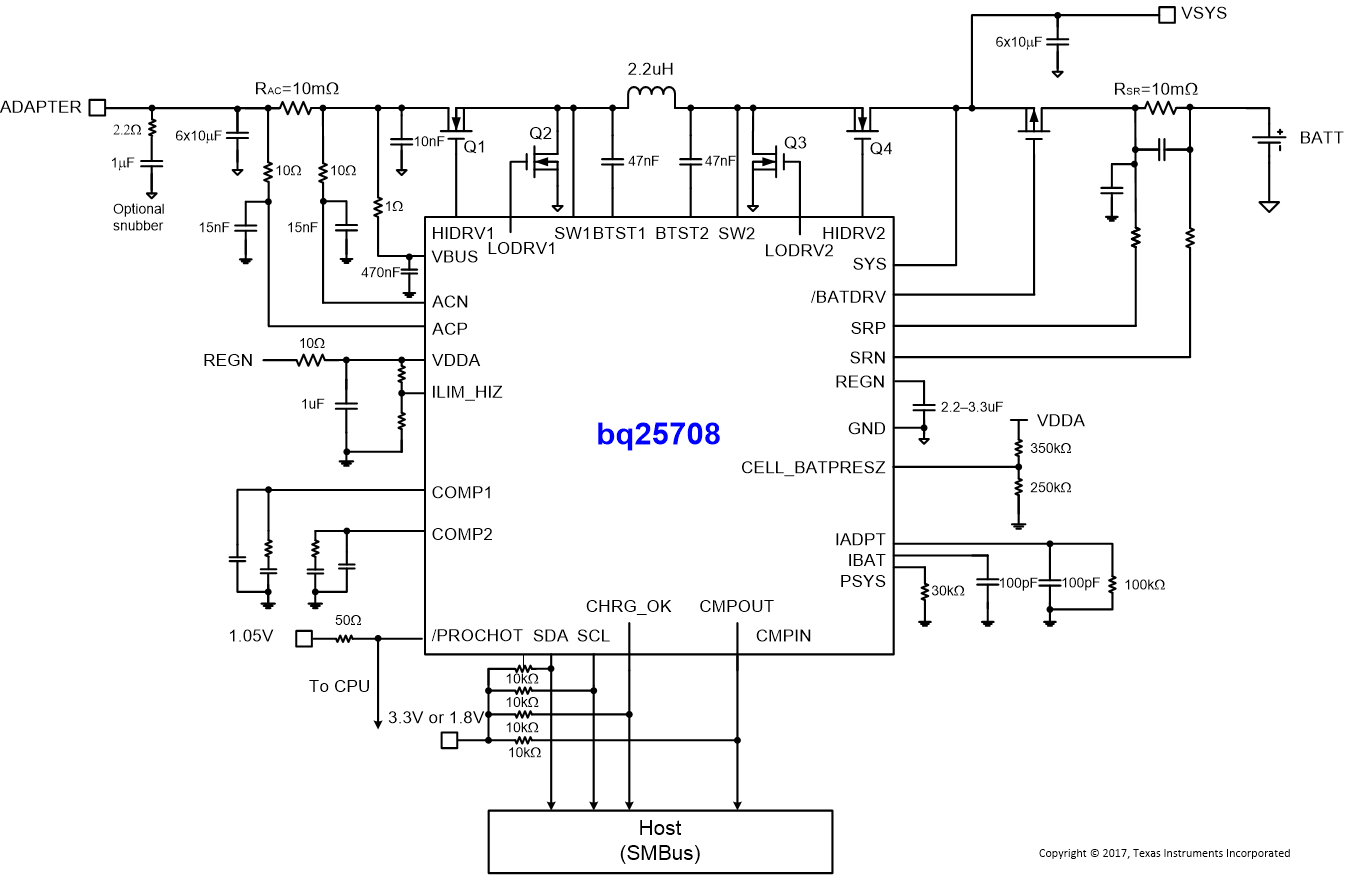 Figure 34. Application Diagram
9.2.1 Design Requirements
| DESIGN PARAMETER | EXAMPLE VALUE |
|---|---|
| Input Voltage(2) | 3.5V < Adapter Voltage < 24V |
| Input Current Limit (2) | 3.2A for 65W adapter |
| Battery Charge Voltage(1) | 8400mV for 2s battery |
| Battery Charge Current(1) | 3072mA for 2s battery |
| Minimum System Voltage(1) | 6144mV for 2s battery |
9.2.2 Detailed Design Procedure
The parameters are configurable using the evaluation software. The simplified application circuit (see Figure 39, as the application diagram) shows the minimum component requirements. Inductor, capacitor, and MOSFET selection are explained in the rest of this section. Refer to the EVM user's guide (SLUUBG6) for the complete application schematic.
9.2.2.1 ACP-ACN Input Filter
The bq25708 has average current mode control. The input current sensing through ACP/ACN is critical to recover inductor current ripple. Parasitic inductance on board will generate high frequency ringing on ACP-ACN which overwhelms converter sensed inductor current information, so it is difficult to manage parasitic inductance created based on different PCB layout. Bigger parasitic inductance will generate bigger sense current ringing which will cause the average current control loop to go into oscillation.
For real system board condition, we suggest to use below circuit design to get best result and filter noise induced from different PCB parasitic factor. With time constant of filter from 47nsec to 200nsec, the filtering on ringing is effective and in the meantime, the delay of on the sensed signal is small and therefore poses no concern for average current mode control.
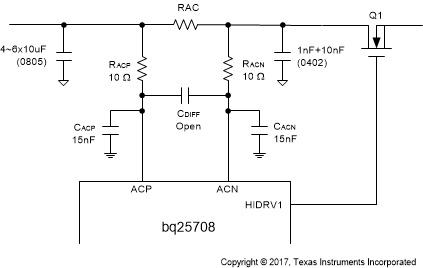 Figure 35. ACN-ACP Input Filter
9.2.2.2 Inductor Selection
The bq25708 has two selectable fixed switching frequency. Higher switching frequency allows the use of smaller inductor and capacitor values. Inductor saturation current should be higher than the charging current (ICHG) plus half the ripple current (IRIPPLE):

The inductor ripple current in buck operation depends on input voltage (VIN), duty cycle (DBUCK = VOUT/VIN), switching frequency (fS) and inductance (L):

During boost operation, the duty cycle is:
DBOOST = 1 – (VBAT/VIN)
and the ripple current is:IRIPPLE_BOOST = DBOOST x fS x VBAT/LBOOST
The maximum inductor ripple current happens with D = 0.5 or close to 0.5. For example, the battery charging voltage range is from 9 V to 12.6 V for 3-cell battery pack. For 20 V adapter voltage, 10 V battery voltage gives the maximum inductor ripple current. Another example is 4-cell battery, the battery voltage range is from 12 V to 16.8 V, and 12 V battery voltage gives the maximum inductor ripple current.
Usually inductor ripple is designed in the range of (20-40%) maximum charging current as a trade-off between inductor size and efficiency for a practical design.
9.2.2.3 Input Capacitor
Bulk input capacitors should be locate in front of input current sensing resistor. Do not recommend to put bulk input capacitors between input sensing resistor and switching MOSFET. Input capacitor should have enough ripple current rating to absorb input switching ripple current. The worst case RMS ripple current is half of the charging current when duty cycle is 0.5 in buck mode. If the converter does not operate at 50% duty cycle, then the worst case capacitor RMS current occurs where the duty cycle is closest to 50% and can be estimated by Equation 5:

Low ESR ceramic capacitor such as X7R or X5R is preferred for input decoupling capacitor and should be placed to the drain of the high side MOSFET and source of the low side MOSFET as close as possible. Voltage rating of the capacitor must be higher than normal input voltage level. 25 V rating or higher capacitor is preferred for 19-20 V input voltage. Minimum 10uF effective capacitance (7 pcs of 10uF 0805 size capacitor) is suggested for 45 W-65 W adapter.
Ceramic capacitors show a dc-bias effect. This effect reduces the effective capacitance when a dc-bias voltage is applied across a ceramic capacitor, as on the input capacitor of a charger. The effect may lead to a significant capacitance drop, especially for high input voltages and small capacitor packages. See the manufacturer's datasheet about the performance with a dc bias voltage applied. It may be necessary to choose a higher voltage rating or nominal capacitance value in order to get the required value at the operating point.
9.2.2.4 Output Capacitor
Output capacitor also should have enough ripple current rating to absorb output switching ripple current. In buck mode the output capacitor RMS current is given:
To get good loop stability, the resonant frequency of the output inductor and output capacitor should be designed between 10 kHz and 20 kHz. The preferred ceramic capacitor is 25V X7R or X5R for output capacitor. Minimum 10uF effective capacitance (7 pcs of 10uF 0805 size capacitor) is suggested to be placed after the Q4 drain, and 50uF effective distributed capacitance on Vsys output. Place minimum 10uF after the charge current sense resistor for best stability.
Ceramic capacitors show a dc-bias effect. This effect reduces the effective capacitance when a dc-bias voltage is applied across a ceramic capacitor, as on the output capacitor of a charger. The effect may lead to a significant capacitance drop, especially for high output voltages and small capacitor packages. See the manufacturer's data sheet about the performance with a dc bias voltage applied. It may be necessary to choose a higher voltage rating or nominal capacitance value in order to get the required value at the operating point.
9.2.2.5 Power MOSFETs Selection
Four external N-channel MOSFETs are used for a synchronous switching battery charger. The gate drivers are internally integrated into the IC with 6V of gate drive voltage. 30 V or higher voltage rating MOSFETs are preferred for 19-20 V input voltage.
Figure-of-merit (FOM) is usually used for selecting proper MOSFET based on a tradeoff between the conduction loss and switching loss. For the top side MOSFET, FOM is defined as the product of a MOSFET's on-resistance, RDS(ON), and the gate-to-drain charge, QGD. For the bottom side MOSFET, FOM is defined as the product of the MOSFET's on-resistance, RDS(ON), and the total gate charge, QG.
The lower the FOM value, the lower the total power loss. Usually lower RDS(ON) has higher cost with the same package size.
The top-side MOSFET loss includes conduction loss and switching loss. It is a function of duty cycle (D=VOUT/VIN), charging current (ICHG), MOSFET's on-resistance (RDS(ON)), input voltage (VIN), switching frequency (fS), turn on time (ton) and turn off time (toff):

The first item represents the conduction loss. Usually MOSFET RDS(ON) increases by 50% with 100°C junction temperature rise. The second term represents the switching loss. The MOSFET turn-on and turn-off times are given by:

where Qsw is the switching charge, Ion is the turn-on gate driving current and Ioff is the turn-off gate driving current. If the switching charge is not given in MOSFET datasheet, it can be estimated by gate-to-drain charge (QGD) and gate-to-source charge (QGS):

Gate driving current can be estimated by REGN voltage (VREGN), MOSFET plateau voltage (Vplt), total turn-on gate resistance (Ron) and turn-off gate resistance (Roff) of the gate driver:

The conduction loss of the bottom-side MOSFET is calculated with the following equation when it operates in synchronous continuous conduction mode:
When charger operates in non-synchronous mode, the bottom-side MOSFET is off. As a result all the freewheeling current goes through the body-diode of the bottom-side MOSFET. The body diode power loss depends on its forward voltage drop (VF), non-synchronous mode charging current (INONSYNC), and duty cycle (D).
The maximum charging current in non-synchronous mode can be up to 0.25 A for a 10 mΩ charging current sensing resistor or 0.5 A if battery voltage is below 2.5 V. The minimum duty cycle happens at lowest battery voltage. Choose the bottom-side MOSFET with either an internal Schottky or body diode capable of carrying the maximum non-synchronous mode charging current.
9.2.3 Application Curves
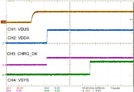
| 2-cell without battery | ||
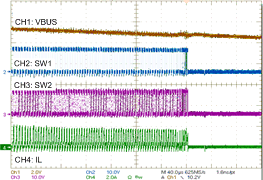
| 3-cell VBAT = 10 V |
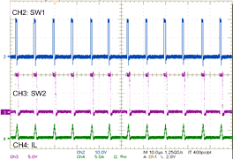
| VBUS = 20 V, VSYS = 10 V, ISYS = 200 mA |
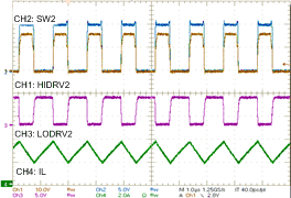
| VBUS = 5 V, VBAT = 10 V |
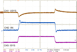
| VBUS = 12 V/3.3 A, 3-cell, VSYS = 9 V, Without battery |
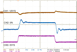
| VBUS = 5 V/3.3 A, 3-cell, VSYS = 9 V, Without battery |
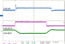
| VBUS = 5 V/3.3 V, VBAT = 7.5 V |
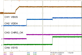
| 2-cell without battery | ||
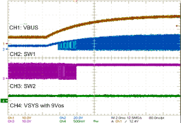
| VBUS 5 V to 20 V |
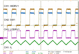
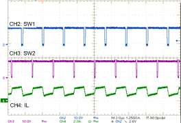
| VBUS = 12 V, VBAT = 12 V |
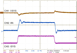
| VBUS = 9 V/3.3 A, 3-cell, VSYS = 9 V, Without battery |
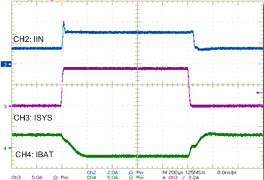
| VBUS = 20 V/3.3 V, VBAT = 7.5 V |