ZHCSNB8A February 2021 – January 2024 BQ25730
PRODUCTION DATA
- 1
- 1 特性
- 2 应用
- 3 说明
- 4 说明(续)
- 5 Device Comparison Table
- 6 Pin Configuration and Functions
- 7 Specifications
-
8 Detailed Description
- 8.1 Overview
- 8.2 Functional Block Diagram
- 8.3
Feature Description
- 8.3.1 Power-Up Sequence
- 8.3.2 Two-Level Battery Discharge Current Limit
- 8.3.3 Fast Role Swap Feature
- 8.3.4 CHRG_OK Indicator
- 8.3.5 Input and Charge Current Sensing
- 8.3.6 Input Voltage and Current Limit Setup
- 8.3.7 Battery Cell Configuration
- 8.3.8 Device HIZ State
- 8.3.9 USB On-The-Go (OTG)
- 8.3.10 Converter Operation
- 8.3.11 Inductance Detection Through IADPT Pin
- 8.3.12 Converter Compensation
- 8.3.13 Continuous Conduction Mode (CCM)
- 8.3.14 Pulse Frequency Modulation (PFM)
- 8.3.15 Switching Frequency and Dithering Feature
- 8.3.16 Current and Power Monitor
- 8.3.17 Input Source Dynamic Power Management
- 8.3.18 Input Current Optimizer (ICO)
- 8.3.19 Two-Level Adapter Current Limit (Peak Power Mode)
- 8.3.20 Processor Hot Indication
- 8.3.21
Device Protection
- 8.3.21.1 Watchdog Timer
- 8.3.21.2 Input Overvoltage Protection (ACOV)
- 8.3.21.3 Input Overcurrent Protection (ACOC)
- 8.3.21.4 System Overvoltage Protection (SYSOVP)
- 8.3.21.5 Battery Overvoltage Protection (BATOVP)
- 8.3.21.6 Battery Discharge Overcurrent Protection (BATOC)
- 8.3.21.7 Battery Short Protection (BATSP)
- 8.3.21.8 System Undervoltage Lockout (VSYS_UVP) and Hiccup Mode
- 8.3.21.9 Thermal Shutdown (TSHUT)
- 8.4 Device Functional Modes
- 8.5 Programming
- 8.6
Register Map
- 8.6.1 ChargeOption0 Register (I2C address = 01/00h) [reset = E70Eh]
- 8.6.2 ChargeCurrent Register (I2C address = 03/02h) [reset = 0000h]
- 8.6.3 ChargeVoltage Register (I2C address = 05/04h) [reset value based on CELL_BATPRESZ pin setting]
- 8.6.4 ChargerStatus Register (I2C address = 21/20h) [reset = 0000h]
- 8.6.5 ProchotStatus Register (I2C address = 23/22h) [reset = B800h]
- 8.6.6 IIN_DPM Register (I2C address = 25/24h) [reset = 4100h]
- 8.6.7 ADCVBUS/PSYS Register (I2C address = 27/26h)
- 8.6.8 ADCIBAT Register (I2C address = 29/28h)
- 8.6.9 ADCIIN/CMPIN Register (I2C address = 2B/2Ah)
- 8.6.10 ADCVSYS/VBAT Register (I2C address = 2D/2Ch)
- 8.6.11 ChargeOption1 Register (I2C address = 31/30h) [reset = 3F00h]
- 8.6.12 ChargeOption2 Register (I2C address = 33/32h) [reset = 00B7]
- 8.6.13 ChargeOption3 Register (I2C address = 35/34h) [reset = 0434h]
- 8.6.14 ProchotOption0 Register (I2C address = 37/36h) [reset = 4A81h(2S~5s) 4A09(1S)]
- 8.6.15 ProchotOption1 Register (I2C address = 39/38h) [reset = 41A0h]
- 8.6.16 ADCOption Register (I2C address = 3B/3Ah) [reset = 2000h]
- 8.6.17 ChargeOption4 Register (I2C address = 3D/3Ch) [reset = 0048h]
- 8.6.18 Vmin Active Protection Register (I2C address = 3F/3Eh) [reset = 006Ch(2s~5s)/0004h(1S)]
- 8.6.19 OTGVoltage Register (I2C address = 07/06h) [reset = 09C4h]
- 8.6.20 OTGCurrent Register (I2C address = 09/08h) [reset = 3C00h]
- 8.6.21 InputVoltage(VINDPM) Register (I2C address = 0B/0Ah) [reset =VBUS-1.28V]
- 8.6.22 VSYS_MIN Register (I2C address = 0D/0Ch) [reset value based on CELL_BATPRESZ pin setting]
- 8.6.23 IIN_HOST Register (I2C address = 0F/0Eh) [reset = 2000h]
- 8.6.24 ID Registers
- 9 Application and Implementation
- 10Power Supply Recommendations
- 11Layout
- 12Device and Documentation Support
- 13Revision History
- 14Mechanical, Packaging, and Orderable Information
8.3.2 Two-Level Battery Discharge Current Limit
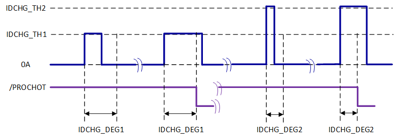
To prevent the triggering of battery overcurrent protection and avoid battery wear-out, two battery current limit levels (IDCHG_TH1 and IDCHG_TH2) PROCHOT profiles are recommended to be enabled. Define IDCHG_TH1 through REG0x39h[7:2], IDCHG_TH2 is set through REG0x3Ch[5:3] for fixed percentage of IDCHG_TH1. There are dedicated de-glitch time setting registers(IDCHG_DEG1 and IDCHG_DEG2) for both IDCHG_TH1 and IDCHG_TH2.
- When battery discharge
current is continuously higher than IDCHG_TH1 for more than IDCHG_DEG1
de-glitch time, PROCHOT is asserted immediately. If the
discharge current reduces to lower than IDCHG_TH1, then the time counter
resets automatically. STAT_IDCHG1 bit will be set to 1 after
PROCHOT is triggered.
Set PP_IDCHG1=1b to enable IDCHG_TH1 for triggering PROCHOT.
- When battery discharge
current is continuously higher than IDCHG_TH2 for more than IDCHG_DEG2
de-glitch time, PROCHOT is asserted immediately. If the
discharge current reduces to lower than IDCHG_TH2, then the time counter
resets automatically. STAT_IDCHG2 bit will be set to 1 after
PROCHOT is triggered.
Set PP_IDCHG2=1b to enable IDCHG_TH2 for triggering PROCHOT.
 Figure 8-1 Two-Level Battery Discharging
Current Trigger PROCHOT Diagram