ZHCSOK3 august 2023 BQ25756
PRODUCTION DATA
- 1
- 1 特性
- 2 应用
- 3 说明
- 4 Revision History
- 5 说明(续)
- 6 Pin Configuration and Functions
- 7 Specifications
-
8 Detailed Description
- 8.1 Overview
- 8.2 Functional Block Diagram
- 8.3
Feature Description
- 8.3.1 Device Power-On-Reset
- 8.3.2 Device Power-Up From Battery Without Input Source
- 8.3.3 Device Power Up from Input Source
- 8.3.4 Battery Charging Management
- 8.3.5 Power Management
- 8.3.6 Reverse Mode Power Direction
- 8.3.7 Integrated 16-Bit ADC for Monitoring
- 8.3.8 Status Outputs (PG, STAT1, STAT2, and INT)
- 8.3.9
Protections
- 8.3.9.1
Voltage and Current Monitoring
- 8.3.9.1.1 VAC Over-voltage Protection (VAC_OVP)
- 8.3.9.1.2 VAC Under-voltage Protection (VAC_UVP)
- 8.3.9.1.3 Battery Over-voltage Protection (BAT_OVP)
- 8.3.9.1.4 Battery Over-current Protection (BAT_OCP)
- 8.3.9.1.5 Reverse Mode Over-voltage Protection (REV_OVP)
- 8.3.9.1.6 Reverse Mode Under-voltage Protection (REV_UVP)
- 8.3.9.1.7 DRV_SUP Under-voltage and Over-voltage Protection (DRV_OKZ)
- 8.3.9.1.8 REGN Under-voltage Protection (REGN_OKZ)
- 8.3.9.2 Thermal Shutdown (TSHUT)
- 8.3.9.1
Voltage and Current Monitoring
- 8.3.10 Serial Interface
- 8.4 Device Functional Modes
- 8.5 BQ25756 Registers
-
9 Application and Implementation
- 9.1 Application Information
- 9.2
Typical Applications
- 9.2.1
Typical Application
- 9.2.1.1 Design Requirements
- 9.2.1.2
Detailed Design Procedure
- 9.2.1.2.1 ACUV / ACOV Input Voltage Operating Window Programming
- 9.2.1.2.2 Charge Voltage Selection
- 9.2.1.2.3 Switching Frequency Selection
- 9.2.1.2.4 Inductor Selection
- 9.2.1.2.5 Input (VAC) Capacitor
- 9.2.1.2.6 Output (VBAT) Capacitor
- 9.2.1.2.7 Sense Resistor (RAC_SNS and RBAT_SNS) and Current Programming
- 9.2.1.2.8 Power MOSFETs Selection
- 9.2.1.2.9 Converter Fast Transient Response
- 9.2.1.3 Application Curves
- 9.2.2 Typical Application (USB-PD EPR Configuration)
- 9.2.1
Typical Application
- 10Power Supply Recommendations
- 11Layout
- 12Device and Documentation Support
- 13Mechanical, Packaging, and Orderable Information
11.2 Layout Example
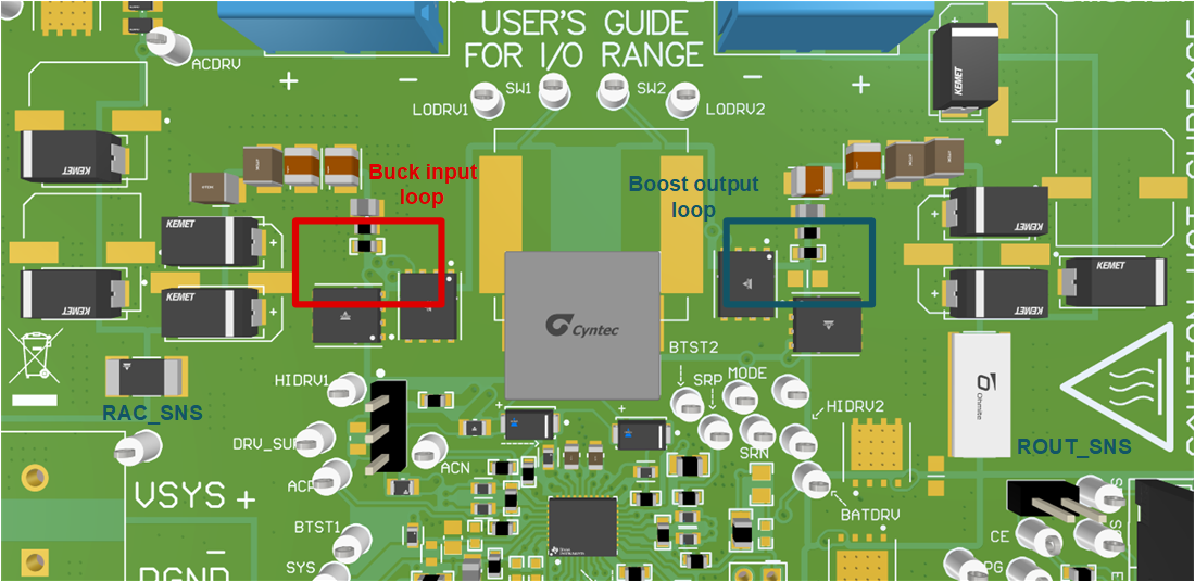
Based on the above layout guidelines, the buck-boost PCB layout example top view is shown below including all the key power components.
 Figure 11-1 PCB Layout Reference Example Top
View
Figure 11-1 PCB Layout Reference Example Top
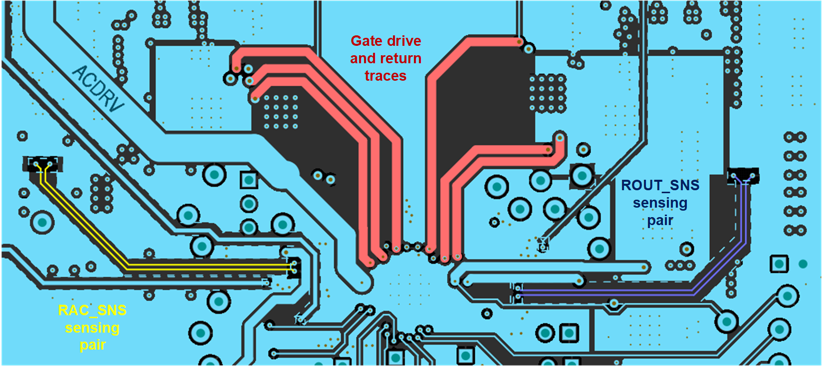
ViewFor both input and output current sensing resistors, differential sensing and routing method are suggested and highlighted in figure below. Use wide trace for gate drive traces, minimum 20-mil trace width. Connect all analog grounds to a dedicated low-impedance copper plane, which is tied to the power ground underneath the IC exposed pad.
 Figure 11-2 PCB Layout Gate Drive and Current Sensing Signal Layer Routing