ZHCSMD3C June 2020 – August 2022 BQ25792
PRODUCTION DATA
- 1 特性
- 2 应用
- 3 说明
- 4 Revision History
- 5 说明(续)
- 6 Device Comparison
- 7 Pin Configuration and Functions
- 8 Specifications
-
9 Detailed Description
- 9.1 Overview
- 9.2 Functional Block Diagram
- 9.3
Feature Description
- 9.3.1 Device Power-On-Reset
- 9.3.2 PROG Pin Configuration
- 9.3.3 Device Power Up from Battery without Input Source
- 9.3.4 Device Power Up from Input Source
- 9.3.5 Dual-Input Power Mux
- 9.3.6 Buck-Boost Converter Operation
- 9.3.7 USB On-The-Go (OTG)
- 9.3.8 Power Path Management
- 9.3.9 Battery Charging Management
- 9.3.10 Integrated 16-Bit ADC for Monitoring
- 9.3.11 Status Outputs ( STAT, and INT)
- 9.3.12 Ship FET Control
- 9.3.13 Protections
- 9.3.14 Serial Interface
- 9.4 Device Functional Modes
- 9.5 Register Map
- 10Application and Implementation
- 11Power Supply Recommendations
- 12Layout
- 13Device and Documentation Support
- 14Mechanical, Packaging, and Orderable Information
9.3.5.4 Two ACFETs-RBFETs
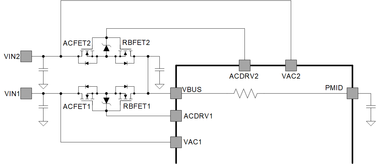
In this scenario, both ACFET1-RBFET1 and ACFET2-RBFET2 are present. VAC1 / VAC2 is tied to the drain of ACFET1 / ACFET2, ACDRV1 / ACDRV2 is connected to the gate of ACFET1 / ACFET2. This structure is developed to support dual-input connected at VAC1 and VAC2. At POR, the charger detects both ACFET1-RBFET1 and ACFET2-RBFET2 present, then updates ACRB1_STAT and ACRB2_STAT to 1.
 Figure 9-4 Two ACFETs-RBFETs Structure
Supporting One Input at VAC1 and One Input at VAC2
Figure 9-4 Two ACFETs-RBFETs Structure
Supporting One Input at VAC1 and One Input at VAC2| PIN OR REGISTER FIELD | STATE |
|---|---|
| External MOSFETs | ACFET1, RBFET1, ACFET2, RBFET2 |
| VAC1 pin | Connected to input source 1 |
| VAC2 pin | Connected to input source 2 |
| ACDRV1 pin | Connected to ACFET1/RBFET1 gate terminals |
| ACDRV2 pin | Connected to ACFET2/RBFET2 gate terminals |
| ACRB1_STAT |
0: ACFET1/RBFET1 Open (Path Disabled)
1: ACFET1/RBFET1 Closed (Path Enabled)
|
| ACRB2_STAT |
0: ACFET2/RBFET2 Open (Path Disabled)
1: ACFET2/RBFET2 Closed (Path Enabled)
|
| DIS_ACDRV |
0: Allow ACDRV1 or ACDRV2 on if all requirements met
1: Force ACDRV1 and ACDRV2 off
|
| EN_ACDRV1 |
0: Force ACDRV1 Off
1: Turn ACDRV1 On if all requirements met
|
| EN_ACDRV2 |
0: Force ACDRV2 Off
1: Turn ACDRV2 On if all requirements met
|
In dual input mode, the ACDRV automatically turns on the ACFET-RBFET of the path where a valid input is first presented, without host intervention. If a valid input is presented on the second path while the first path is already on with a valid input, the ACFET-RBFET of the second path remains off. If desired, the host may manually perform a switch between power paths by switching the values of EN_ACDRV1 and EN_ACDRV2. Both EN_ACDRV bits may be updated in a single I2C write operation to minimize the transition time. Note that programming EN_ACDRV1 = 1, EN_ACDRV2 = 1 at the same time to turn on both ACFET1-RBFET1 and ACFET2-RBFET2 is not allowed, and will be ignored by the charger.
To transition from one input to the other, the device first turns off the initially active ACFET-RBFET pair, waits until the VBUS voltage drops lower than VBUS_PRESENT, and then enables the new ACFET-RBFET pair. During this change over, the converter stops switching for a short period of time. When no battery is present or the battery is depleted, the system output will fall. The user has to be aware of this and avoid the input source swap when the battery voltage is too low.
If two valid voltages are present at VAC1 and VAC2 and the source on the connected path becomes invalid because of VAC_UVLO, VAC_OV or IBUS_OC, the charger automatically swaps the input without any host engagement. Any time that the converter autonomously swaps the source paths, it will also update the EN_ACDRV1 and EN_ACDRV2 bits accordingly in order to indicate the active power path.
With only one valid input presented at either VAC1 or VAC2, the ACFET1-RBFET1 and ACFET2-RBFET2 can not be both turned off by setting REG0x13[7:6] = 00. Instead, the host should set DIS_ACDRV = 1 to force both ACFET-RBFET pairs off. With input sources present at both VAC1 and VAC2, the host can turn off the two ACFET-RBFET pairs by setting either REG0x13[7:6] = 00 or DIS_ACDRV = 1.