ZHCSNY0B May 2020 – January 2023 BQ25798
PRODUCTION DATA
- 1 特性
- 2 应用
- 3 说明
- 4 Revision History
- 5 说明(续)
- 6 Device Comparison
- 7 Pin Configuration and Functions
- 8 Specifications
-
9 Detailed Description
- 9.1 Overview
- 9.2 Functional Block Diagram
- 9.3
Feature Description
- 9.3.1 Device Power-On-Reset
- 9.3.2 PROG Pin Configuration
- 9.3.3 Device Power Up from Battery without Input Source
- 9.3.4 Device Power Up from Input Source
- 9.3.5 Dual-Input Power Mux
- 9.3.6 Buck-Boost Converter Operation
- 9.3.7 USB On-The-Go (OTG)
- 9.3.8 Power Path Management
- 9.3.9 Battery Charging Management
- 9.3.10 Integrated 16-Bit ADC for Monitoring
- 9.3.11 Status Outputs ( STAT, and INT)
- 9.3.12 Ship FET Control
- 9.3.13
Protections
- 9.3.13.1
Voltage and Current Monitoring
- 9.3.13.1.1 VAC Over-voltage Protection (VAC_OVP)
- 9.3.13.1.2 VBUS Over-voltage Protection (VBUS_OVP)
- 9.3.13.1.3 VBUS Under-voltage Protection (POORSRC)
- 9.3.13.1.4 System Over-voltage Protection (VSYS_OVP)
- 9.3.13.1.5 System Short Protection (VSYS_SHORT)
- 9.3.13.1.6 Battery Over-voltage Protection (VBAT_OVP)
- 9.3.13.1.7 Battery Over-current Protection (IBAT_OCP)
- 9.3.13.1.8 Input Over-current Protection (IBUS_OCP)
- 9.3.13.1.9 OTG Over-voltage Protection (OTG_OVP)
- 9.3.13.1.10 OTG Under-voltage Protection (OTG_UVP)
- 9.3.13.2 Thermal Regulation and Thermal Shutdown
- 9.3.13.1
Voltage and Current Monitoring
- 9.3.14 Serial Interface
- 9.4 Device Functional Modes
- 9.5 Register Map
- 10Application and Implementation
- 11Power Supply Recommendations
- 12Layout
- 13Device and Documentation Support
- 14Mechanical, Packaging, and Orderable Information
9.3.5.3 One ACFET-RBFET
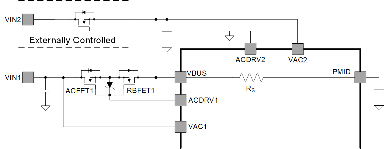
In this configuration, only ACFET1-RBFET1 is present, ACFET2-RBFET2 is not. VAC1 is tied to the drain of ACFET1, ACDRV1 is connected to the gates of ACFET1 and RBFET1. VAC2 is shorted to VBUS, ACDRV2 is pulled down to GND. This structure is illustrated in #GUID-5982433D-1524-4DBE-A995-8E608B2B2B65, which is able to support either single input (one from VAC1 to VBUS through ACFET1-RBFET1) or dual-input (one from VAC1 to VBUS through ACFET1-RBFET1, the other one connected directly to VBUS) applications. At POR, the charger detects only ACFET1-RBFET1 present and configures the power mux register fields as shown in Table 9-7.
 Figure 9-3 One ACFET-RBFET Structure
Supporting One Input at VAC1 and/or One Input at VBUS
Figure 9-3 One ACFET-RBFET Structure
Supporting One Input at VAC1 and/or One Input at VBUS| PIN OR REGISTER FIELD | STATE |
|---|---|
| External MOSFETs | ACFET1 and RBFET1 only |
| VAC1 | Connected to input source 1 |
| VAC2 | Shorted to VBUS |
| ACDRV1 | Connected to ACFET1/RBFET1 gate terminals |
| ACDRV2 | Shorted to GND |
| ACRB1_STAT |
0: ACFET1/RBFET1 Open (Path Disabled)
1: ACFET1/RBFET1 Closed (Path Enabled)
|
| ACRB2_STAT | 0 (Read Only) |
| DIS_ACDRV |
0: Allow ACDRV1 On if all requirements met
1: Force ACDRV1 Off
|
| EN_ACDRV1 |
0: Force ACDRV1 Off
1: Turn ACDRV1 On if all requirements met
|
| EN_ACDRV2 | Locked at 0 |
When a valid input is presented at VAC1, the charger will set EN_ACDRV1 = 1 and turn ACFET1-RBFET1 on. To swap from the input at VAC1 to the input at VBUS, the host has to turn off the ACFET1-RBFET1 first by setting DIS_ACDRV=1 (forcing EN_ACDRV1 = 0), then enable the other input source which is connected directly to VBUS. To swap from the input at VBUS to the input at VAC1, the host has to disable the input source connected to VBUS, wait for VBUS to fall below VBUS_PRESENT, then turn on the ACFET1-RBFET1 by setting DIS_ACDRV = 0.