ZHCSNY0B May 2020 – January 2023 BQ25798
PRODUCTION DATA
- 1 特性
- 2 应用
- 3 说明
- 4 Revision History
- 5 说明(续)
- 6 Device Comparison
- 7 Pin Configuration and Functions
- 8 Specifications
-
9 Detailed Description
- 9.1 Overview
- 9.2 Functional Block Diagram
- 9.3
Feature Description
- 9.3.1 Device Power-On-Reset
- 9.3.2 PROG Pin Configuration
- 9.3.3 Device Power Up from Battery without Input Source
- 9.3.4 Device Power Up from Input Source
- 9.3.5 Dual-Input Power Mux
- 9.3.6 Buck-Boost Converter Operation
- 9.3.7 USB On-The-Go (OTG)
- 9.3.8 Power Path Management
- 9.3.9 Battery Charging Management
- 9.3.10 Integrated 16-Bit ADC for Monitoring
- 9.3.11 Status Outputs ( STAT, and INT)
- 9.3.12 Ship FET Control
- 9.3.13
Protections
- 9.3.13.1
Voltage and Current Monitoring
- 9.3.13.1.1 VAC Over-voltage Protection (VAC_OVP)
- 9.3.13.1.2 VBUS Over-voltage Protection (VBUS_OVP)
- 9.3.13.1.3 VBUS Under-voltage Protection (POORSRC)
- 9.3.13.1.4 System Over-voltage Protection (VSYS_OVP)
- 9.3.13.1.5 System Short Protection (VSYS_SHORT)
- 9.3.13.1.6 Battery Over-voltage Protection (VBAT_OVP)
- 9.3.13.1.7 Battery Over-current Protection (IBAT_OCP)
- 9.3.13.1.8 Input Over-current Protection (IBUS_OCP)
- 9.3.13.1.9 OTG Over-voltage Protection (OTG_OVP)
- 9.3.13.1.10 OTG Under-voltage Protection (OTG_UVP)
- 9.3.13.2 Thermal Regulation and Thermal Shutdown
- 9.3.13.1
Voltage and Current Monitoring
- 9.3.14 Serial Interface
- 9.4 Device Functional Modes
- 9.5 Register Map
- 10Application and Implementation
- 11Power Supply Recommendations
- 12Layout
- 13Device and Documentation Support
- 14Mechanical, Packaging, and Orderable Information
9.3.11.2 Interrupt to Host ( INT)
In some applications, the host does not always monitor charger operation. The INT pin notifies the system host on the device operation. By default, the following events generate an active-low, 256µs INT pulse.
- Good input source detected
- VVBUS < VVBUS_OVP threshold
- VVBUS > VPOORSRC (typical 3.4 V) when IPOORSRC (typical 30 mA) current is applied (not a poor source)
- VBUS_STAT changes state (VBUS_STAT any bit change)
- Good input source removed
- Entering IINDPM regulation
- Entering VINDPM regulation
- Entering IC junction temperature regulation (TREG)
- I2C Watchdog timer expired
- At initial power up, this INT gets asserted to signal I2C is ready for communication
- Charger status changes state (CHRG_STAT value change), including Charge Complete
- TS_STAT changes state (TS_STAT any bit change)
- VBUS over-voltage detected (VBUS_OVP)
- VAC over-voltage detected (VAC_OVP for VAC1 or VAC2)
- Junction temperature shutdown (TSHUT)
- Battery over-voltage detected (BATOVP)
- System over-voltage detected (VSYS_OVP)
- IBUS over-current detected (IBUS_OCP)
- IBAT over-current detected (IBAT_OCP)
- Charge safety timer expired, including trickle charge and pre-charge and fast charge safety timer expired
- A rising edge on any of the other *_STAT bits
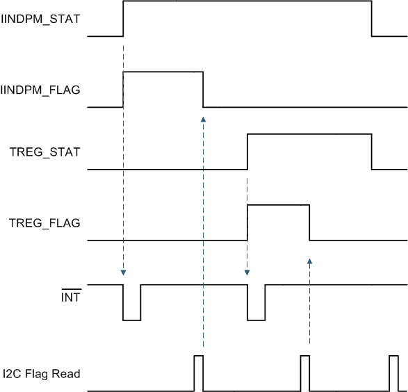
Each one of these INT sources can be masked off to prevent INT pulses from being sent out when they occur. Three bits exist for each one of these events:
- The STAT bit holds the current status of each INT source
- The FLAG bit holds information on which source produced an INT, regardless of the current status
- The MASK bit is used to prevent the device from sending out INT for each particular event
When one of the above conditions occurs (a rising edge on any of the *_STAT bits), the device sends out an INT pulse and keeps track of which source generated the INT via the FLAG registers. The FLAG register bits are automatically reset to zero after the host reads them, and a new edge on STAT bit is required to re-assert the FLAG. This sequence is illustrated in #T4885767-152.
 Figure 9-14 INT
Generation Behavior Example