ZHCSNY0B May 2020 – January 2023 BQ25798
PRODUCTION DATA
- 1 特性
- 2 应用
- 3 说明
- 4 Revision History
- 5 说明(续)
- 6 Device Comparison
- 7 Pin Configuration and Functions
- 8 Specifications
-
9 Detailed Description
- 9.1 Overview
- 9.2 Functional Block Diagram
- 9.3
Feature Description
- 9.3.1 Device Power-On-Reset
- 9.3.2 PROG Pin Configuration
- 9.3.3 Device Power Up from Battery without Input Source
- 9.3.4 Device Power Up from Input Source
- 9.3.5 Dual-Input Power Mux
- 9.3.6 Buck-Boost Converter Operation
- 9.3.7 USB On-The-Go (OTG)
- 9.3.8 Power Path Management
- 9.3.9 Battery Charging Management
- 9.3.10 Integrated 16-Bit ADC for Monitoring
- 9.3.11 Status Outputs ( STAT, and INT)
- 9.3.12 Ship FET Control
- 9.3.13
Protections
- 9.3.13.1
Voltage and Current Monitoring
- 9.3.13.1.1 VAC Over-voltage Protection (VAC_OVP)
- 9.3.13.1.2 VBUS Over-voltage Protection (VBUS_OVP)
- 9.3.13.1.3 VBUS Under-voltage Protection (POORSRC)
- 9.3.13.1.4 System Over-voltage Protection (VSYS_OVP)
- 9.3.13.1.5 System Short Protection (VSYS_SHORT)
- 9.3.13.1.6 Battery Over-voltage Protection (VBAT_OVP)
- 9.3.13.1.7 Battery Over-current Protection (IBAT_OCP)
- 9.3.13.1.8 Input Over-current Protection (IBUS_OCP)
- 9.3.13.1.9 OTG Over-voltage Protection (OTG_OVP)
- 9.3.13.1.10 OTG Under-voltage Protection (OTG_UVP)
- 9.3.13.2 Thermal Regulation and Thermal Shutdown
- 9.3.13.1
Voltage and Current Monitoring
- 9.3.14 Serial Interface
- 9.4 Device Functional Modes
- 9.5 Register Map
- 10Application and Implementation
- 11Power Supply Recommendations
- 12Layout
- 13Device and Documentation Support
- 14Mechanical, Packaging, and Orderable Information
9.4.1 Host Mode and Default Mode
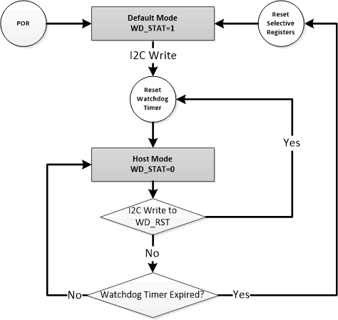
The device is a host controlled charger, but it can operate in default mode without host management. In default mode, the device can be used as an autonomous charger with no host or while host is in sleep mode. When the charger is in default mode, WD_STAT bit becomes HIGH, WD_FLAG is set to 1, and an INT is asserted low to alert the host (unless masked by WD_MASK). The WD_FLAG bit would read as 1 upon the first read and then 0 upon subsequent reads. When the charger is in host mode, WD_STAT bit is LOW.
After power-on-reset, the device starts in default mode with watchdog timer expired. All the registers are in the default settings.
In default mode, the device keeps charging the battery with default 1-hour trickle charging safety timer, 2-hour pre-charging safety timer and the 12-hour fast charging safety timer. At the end of the 1-hour or 2-hour or 12-hour timer expired, the charging is stopped and the buck-boost converter continues to operate to supply system load.
A write to any I2C register transitions the charger from default mode to host mode, and initiates the watchdog timer. All the device parameters can be programmed by the host. To keep the device in host mode, the host has to reset the watchdog timer by writing 1 to WD_RST bit before the watchdog timer expires (WD_STAT bit is set), or disable watchdog timer by setting WATCHDOG bits = 00.
When the watchdog timer is expired, the device returns to default mode and all registers are reset to default values except the ones described in GUID-AE2BDEB6-B207-4010-9B7A-F10CCB3793B1.html. The watchdog timer will be reset on any write if the watchdog timer has expired. When watchdog timer expires, WD_STAT and WD_FLAG is set to 1, and an INT is asserted low to alert the host (unless masked by WD_MASK).
 Figure 9-25 Watchdog Timer Flow
Chart