SLUSFH5A May 2024 – October 2024 BQ25856-Q1
PRODUCTION DATA
- 1
- 1 Features
- 2 Applications
- 3 Description
- 4 Device Comparison
- 5 Pin Configuration and Functions
- 6 Specifications
-
7 Detailed Description
- 7.1 Overview
- 7.2 Functional Block Diagram
- 7.3
Feature Description
- 7.3.1 Device Power-On-Reset
- 7.3.2 Device Power-Up From Battery Without Input Source
- 7.3.3 Device Power Up From Input Source
- 7.3.4 Battery Charging Management
- 7.3.5 Power Management
- 7.3.6 Switching Frequency Dithering Feature
- 7.3.7 Reverse Mode Power Direction
- 7.3.8 Integrated 16-Bit ADC for Monitoring
- 7.3.9 Status Outputs (PG, STAT1, STAT2, and INT)
- 7.3.10
Protections
- 7.3.10.1
Voltage and Current Monitoring
- 7.3.10.1.1 VAC Over-voltage Protection (VAC_OVP)
- 7.3.10.1.2 VAC Under-voltage Protection (VAC_UVP)
- 7.3.10.1.3 Battery Over-voltage Protection (BAT_OVP)
- 7.3.10.1.4 Battery Over-current Protection (BAT_OCP)
- 7.3.10.1.5 Reverse Mode Over-voltage Protection (REV_OVP)
- 7.3.10.1.6 Reverse Mode Under-voltage Protection (REV_UVP)
- 7.3.10.1.7 DRV_SUP Under-voltage and Over-voltage Protection (DRV_OKZ)
- 7.3.10.1.8 REGN Under-voltage Protection (REGN_OKZ)
- 7.3.10.2 Thermal Shutdown (TSHUT)
- 7.3.10.1
Voltage and Current Monitoring
- 7.3.11 Serial Interface
- 7.4 Device Functional Modes
- 7.5 BQ25856-Q1 Registers
-
8 Application and Implementation
- 8.1 Application Information
- 8.2
Typical Applications
- 8.2.1
Typical Application
- 8.2.1.1 Design Requirements
- 8.2.1.2
Detailed Design Procedure
- 8.2.1.2.1 ACUV / ACOV Input Voltage Operating Window Programming
- 8.2.1.2.2 Charge Voltage Selection
- 8.2.1.2.3 Switching Frequency Selection
- 8.2.1.2.4 Inductor Selection
- 8.2.1.2.5 Input (VAC) Capacitor
- 8.2.1.2.6 Output (VBAT) Capacitor
- 8.2.1.2.7 Sense Resistor (RAC_SNS and RBAT_SNS) and Current Programming
- 8.2.1.2.8 Power MOSFETs Selection
- 8.2.1.2.9 Converter Fast Transient Response
- 8.2.1.3 Application Curves
- 8.2.2 Typical Application (4s LiFePO4 car battery configuration)
- 8.2.3 Typical Application (Capacitor Backup)
- 8.2.1
Typical Application
- 9 Power Supply Recommendations
- 10Layout
- 11Device and Documentation Support
- 12Revision History
- 13Mechanical, Packaging, and Orderable Information
封装选项
请参考 PDF 数据表获取器件具体的封装图。
机械数据 (封装 | 引脚)
- RRV|36
散热焊盘机械数据 (封装 | 引脚)
- RRV|36
订购信息
7.4.1 Host Mode and Default Mode
The device is a host controlled charger, but it can operate in default mode without host management. In default mode, the device can be used as an autonomous charger with no host or while host is in sleep mode. When the charger is in default mode, WD_STAT bit becomes HIGH, WD_FLAG is set to 1, and a INT is asserted low to alert the host (unless masked by WD_MASK). The WD_FLAG bit would read as a '1' upon the first read and then '0' upon subsequent reads. When the charger is in host mode, WD_STAT bit is LOW.
After power-on-reset, the device starts in default mode with watchdog timer expired. All the registers are in the default settings.
In default mode, the device keeps charging the battery with default 2-hour pre-charging safety timer and the 12-hour fast charging safety timer. At the end of the 2-hour or 12-hour timer expiration, the charging is stopped if termination has not been detected.
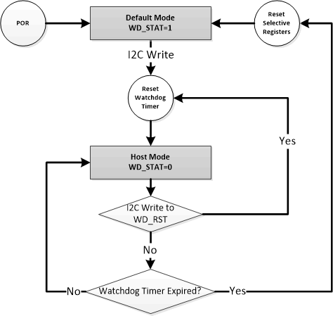
A write to any I2C register transitions the charger from default mode to host mode, and initiates the watchdog timer. All the device parameters can be programmed by the host. To keep the device in host mode, the host has to reset the watchdog timer by writing 1 to WD_RST bit before the watchdog timer expires (WD_STAT bit is set), or disable watchdog timer by setting WATCHDOG bits = 00.
When the watchdog timer is expired, the device returns to default mode and select registers are reset to default values as detailed in the Register Map section. The Watchdog timer will be reset on any write if the watchdog timer has expired. When watchdog timer expires, WD_STAT and WD_FLAG is set to 1, and /INT is asserted low to alert the host (unless masked by WD_MASK).
 Figure 7-15 Watchdog Timer
Flow Chart