SLUSFH5A May 2024 – October 2024 BQ25856-Q1
PRODUCTION DATA
- 1
- 1 Features
- 2 Applications
- 3 Description
- 4 Device Comparison
- 5 Pin Configuration and Functions
- 6 Specifications
-
7 Detailed Description
- 7.1 Overview
- 7.2 Functional Block Diagram
- 7.3
Feature Description
- 7.3.1 Device Power-On-Reset
- 7.3.2 Device Power-Up From Battery Without Input Source
- 7.3.3 Device Power Up From Input Source
- 7.3.4 Battery Charging Management
- 7.3.5 Power Management
- 7.3.6 Switching Frequency Dithering Feature
- 7.3.7 Reverse Mode Power Direction
- 7.3.8 Integrated 16-Bit ADC for Monitoring
- 7.3.9 Status Outputs (PG, STAT1, STAT2, and INT)
- 7.3.10
Protections
- 7.3.10.1
Voltage and Current Monitoring
- 7.3.10.1.1 VAC Over-voltage Protection (VAC_OVP)
- 7.3.10.1.2 VAC Under-voltage Protection (VAC_UVP)
- 7.3.10.1.3 Battery Over-voltage Protection (BAT_OVP)
- 7.3.10.1.4 Battery Over-current Protection (BAT_OCP)
- 7.3.10.1.5 Reverse Mode Over-voltage Protection (REV_OVP)
- 7.3.10.1.6 Reverse Mode Under-voltage Protection (REV_UVP)
- 7.3.10.1.7 DRV_SUP Under-voltage and Over-voltage Protection (DRV_OKZ)
- 7.3.10.1.8 REGN Under-voltage Protection (REGN_OKZ)
- 7.3.10.2 Thermal Shutdown (TSHUT)
- 7.3.10.1
Voltage and Current Monitoring
- 7.3.11 Serial Interface
- 7.4 Device Functional Modes
- 7.5 BQ25856-Q1 Registers
-
8 Application and Implementation
- 8.1 Application Information
- 8.2
Typical Applications
- 8.2.1
Typical Application
- 8.2.1.1 Design Requirements
- 8.2.1.2
Detailed Design Procedure
- 8.2.1.2.1 ACUV / ACOV Input Voltage Operating Window Programming
- 8.2.1.2.2 Charge Voltage Selection
- 8.2.1.2.3 Switching Frequency Selection
- 8.2.1.2.4 Inductor Selection
- 8.2.1.2.5 Input (VAC) Capacitor
- 8.2.1.2.6 Output (VBAT) Capacitor
- 8.2.1.2.7 Sense Resistor (RAC_SNS and RBAT_SNS) and Current Programming
- 8.2.1.2.8 Power MOSFETs Selection
- 8.2.1.2.9 Converter Fast Transient Response
- 8.2.1.3 Application Curves
- 8.2.2 Typical Application (4s LiFePO4 car battery configuration)
- 8.2.3 Typical Application (Capacitor Backup)
- 8.2.1
Typical Application
- 9 Power Supply Recommendations
- 10Layout
- 11Device and Documentation Support
- 12Revision History
- 13Mechanical, Packaging, and Orderable Information
封装选项
请参考 PDF 数据表获取器件具体的封装图。
机械数据 (封装 | 引脚)
- RRV|36
散热焊盘机械数据 (封装 | 引脚)
- RRV|36
订购信息
10.2 Layout Example
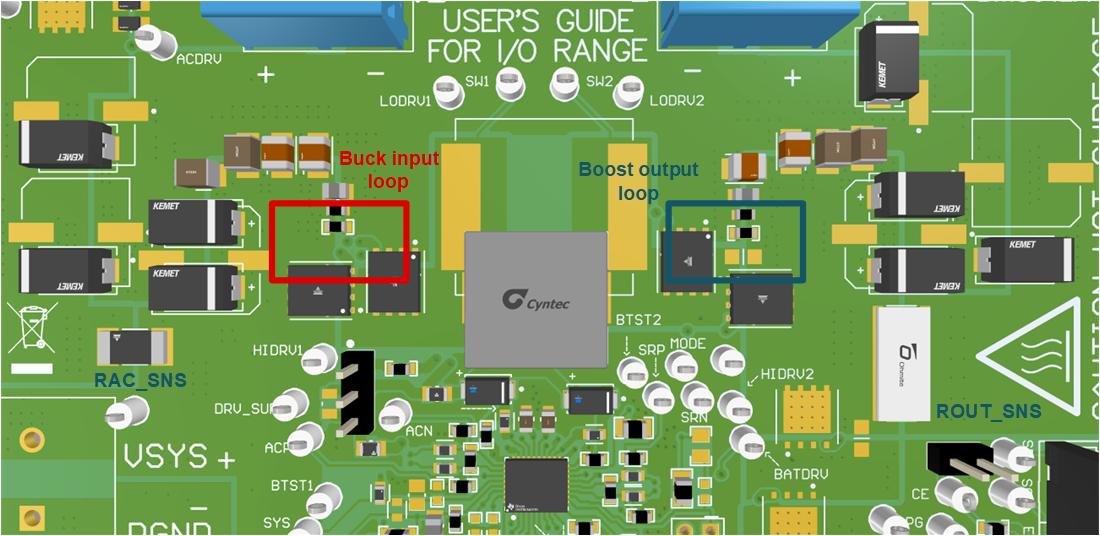
Based on the above layout guidelines, the buck-boost PCB layout example top view is shown below including all the key power components.
 Figure 10-1 PCB Layout Reference Example Top
View
Figure 10-1 PCB Layout Reference Example Top
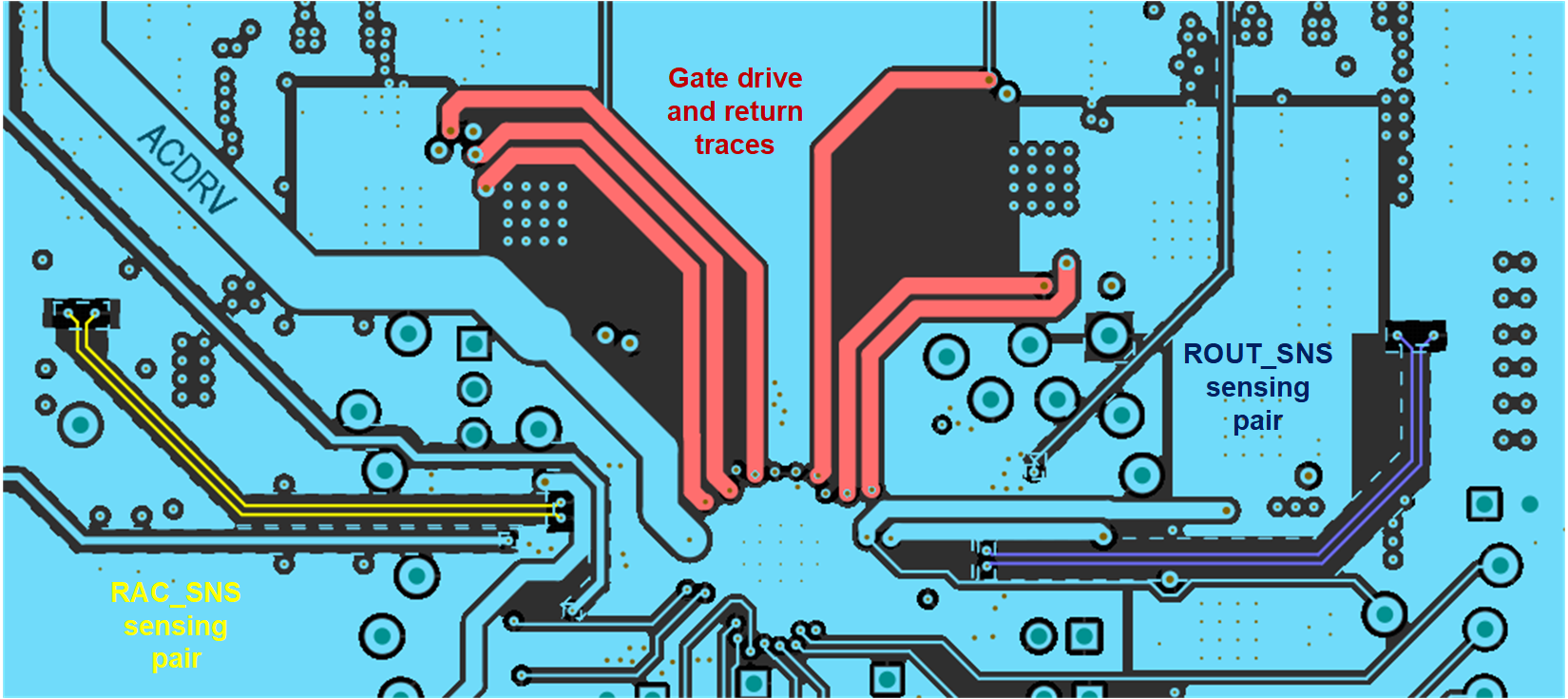
ViewFor both input and output current sensing resistors, differential sensing and routing method are suggested and highlighted in figure below. Use wide trace for gate drive traces, minimum 20-mil trace width. Connect all analog grounds to a dedicated low-impedance copper plane, which is tied to the power ground underneath the IC exposed pad.
 Figure 10-2 PCB Layout Gate Drive and Current Sensing Signal Layer Routing