ZHCSJI9A March   2019  – June 2019 BQ25886

PRODUCTION DATA.  

  1. 特性
  2. 应用
  3. 说明
    1.     简化原理图
  4. 修订历史记录
  5. Device Comparison Table
  6. Pin Configuration and Functions
    1.     Pin Functions
  7. Specifications
    1. 7.1 Absolute Maximum Ratings
    2. 7.2 ESD Ratings
    3. 7.3 Recommended Operating Conditions
    4. 7.4 Thermal Information
    5. 7.5 Electrical Characteristics
    6. 7.6 Timing Requirements
    7. 7.7 Typical Characteristics
  8. Detailed Description
    1. 8.1 Overview
    2. 8.2 Functional Block Diagram
    3. 8.3 Feature Description
      1. 8.3.1  Device Power-On-Reset
      2. 8.3.2  Device Power Up from Battery without Input Source
      3. 8.3.3  Device Power Up from Input Source
        1. 8.3.3.1 Poor Source Qualification
        2. 8.3.3.2 Input Source Type Detection
          1. 8.3.3.2.1 D+/D– Detection Sets Input Current Limit
        3. 8.3.3.3 Power Up REGN Regulator (LDO)
        4. 8.3.3.4 Converter Power Up
      4. 8.3.4  Input Current Optimizer (ICO)
      5. 8.3.5  Buck Mode Operation from Battery (OTG)
      6. 8.3.6  PowerPath Management
        1. 8.3.6.1 Narrow VDC Architecture
        2. 8.3.6.2 Dynamic Power Management
        3. 8.3.6.3 Supplement Mode
      7. 8.3.7  Battery Charging Management
        1. 8.3.7.1 Autonomous Charging Cycle
        2. 8.3.7.2 Battery Charging Profile
        3. 8.3.7.3 Charging Termination
        4. 8.3.7.4 Thermistor Qualification
          1. 8.3.7.4.1 JEITA Guideline Compliance in Charge Mode
        5. 8.3.7.5 Charging Safety Timer
      8. 8.3.8  Status Outputs
        1. 8.3.8.1 Power Good Indicator (PG)
        2. 8.3.8.2 Charging Status Indicator (STAT)
      9. 8.3.9  Input Current Limit on ILIM Pin
      10. 8.3.10 Voltage and Current Monitoring
        1. 8.3.10.1 Voltage and Current Monitoring in Boost Mode
          1. 8.3.10.1.1 Input Over-Voltage Protection
          2. 8.3.10.1.2 Input Under-Voltage Protection
          3. 8.3.10.1.3 System Over-Voltage Protection
          4. 8.3.10.1.4 System Over-Current Protection
        2. 8.3.10.2 Voltage and Current Monitoring in OTG Buck Mode
          1. 8.3.10.2.1 VBUS Over-voltage Protection
          2. 8.3.10.2.2 VBUS Over-Current Protection
      11. 8.3.11 Thermal Regulation and Thermal Shutdown
        1. 8.3.11.1 Thermal Protection in Boost Mode
        2. 8.3.11.2 Thermal Protection in OTG Buck Mode
      12. 8.3.12 Battery Protection
        1. 8.3.12.1 Battery Over-Voltage Protection (BATOVP)
    4. 8.4 Device Functional Modes
  9. Application and Implementation
    1. 9.1 Application Information
    2. 9.2 Typical Application
      1. 9.2.1 Design Requirements
      2. 9.2.2 Detailed Design Procedure
        1. 9.2.2.1 Inductor Selection
        2. 9.2.2.2 Input (VBUS / PMID) Capacitor
        3. 9.2.2.3 Output (VSYS) Capacitor
        4. 9.2.2.4 ILIM resistor
        5. 9.2.2.5 ICHGSET resistor
      3. 9.2.3 Application Curves
  10. 10Power Supply Recommendations
  11. 11Layout
    1. 11.1 Layout Guidelines
    2. 11.2 Layout Example
  12. 12器件和文档支持
    1. 12.1 器件支持
      1. 12.1.1 第三方米6体育平台手机版_好二三四免责声明
    2. 12.2 文档支持
      1. 12.2.1 相关文档
    3. 12.3 接收文档更新通知
    4. 12.4 社区资源
    5. 12.5 商标
    6. 12.6 静电放电警告
    7. 12.7 Glossary
  13. 13机械、封装和可订购信息

封装选项

机械数据 (封装 | 引脚)
散热焊盘机械数据 (封装 | 引脚)
订购信息

JEITA Guideline Compliance in Charge Mode

To improve the safety of charging Li-ion batteries, JEITA guideline was released on April 20, 2007. The guideline emphasized the importance of avoiding a high charge current and high charge voltage at certain low and high temperature ranges.

To initiate a charge cycle, the voltage on TS pin must be within the VT1 to VT5 thresholds. If TS voltage exceeds the T1-T5 range, the controller suspends charging and waits until the battery temperature is within the T1 to T5 range. At cool temperature (T1-T2), JEITA recommends the charge current to be reduced to half of the charge current or lower. At warm temperature (T3-T5), JEITA recommends charge voltage less than 4.1 V / cell.

On the BQ25886, at cool temperature (T1-T2), the charge current is reduced to 20% of the fast charge current, ICHG. At warm temperature (T3 - T5), the charge voltage is set to 8.0 V. Whenever the charger detectes "warm" or "cool" temperature, termination is automatically disabled.
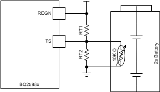
BQ25886 slvse40_ts_resistor_network.gifFigure 18. TS Resistor Network
BQ25886 TS_Charging_Values_886.gif
Figure 19. TS Charging Values

Assuming a 103AT NTC (Negative Temperature Coefficient) thermistor on the battery pack as shown above, the value of RT1 and RT2 can be determined by:

Equation 1. BQ25886 RT2_eqn1_SLUSDL3.gif
Equation 2. BQ25886 RT1_eqn2_SLUSDL3.gif

Select 0°C to 60°C range for Li-ion or Li-polymer battery:

RNTC,T1 = 27.28 kΩ

RNTC,T5 = 3.02 kΩ

RT1 = 5.24 kΩ

RT2 = 30.31 kΩ