| QUIESCENT CURRENTS |
| IBAT |
Battery discharge current (BAT, SW, SYS) in buck mode |
VBAT = 4.2 V, V(VBUS) < V(UVLO), leakage between BAT and VBUS |
|
|
5 |
µA |
| High-Z Mode, No VBUS, BATFET Disabled (REG09[5] = 1), Battery Monitor Disabled, TJ < 85°C |
|
12 |
23 |
µA |
| High-Z Mode, No VBUS, BATFET Enabled (REG09[5] = 0), Battery Monitor Disabled, TJ < 85°C |
|
32 |
60 |
µA |
| I(VBUS_HIZ) |
Input supply current (VBUS) in buck mode when High-Z mode is enabled |
V(VBUS)= 5 V, High-Z Mode, No Battery, Battery Monitor Disabled |
|
15 |
35 |
µA |
| V(VBUS)= 12 V, High-Z Mode, No Battery, Battery Monitor Disabled |
|
25 |
50 |
µA |
| I(VBUS) |
Input supply current (VBUS) in buck mode |
VBUS > V(UVLO), VBUS > VBAT, Converter not switching |
|
1.5 |
3 |
mA |
| VBUS > V(UVLO), VBUS > VBAT, Converter switching, VBAT = 3.2V, ISYS = 0A |
|
3 |
|
mA |
| VBUS > V(UVLO), VBUS > VBAT, Converter switching, VBAT = 3.8 V, ISYS = 0 A |
|
3 |
|
mA |
| I(BOOST) |
Battery discharge current in boost mode |
VBAT = 4.2 V, Boost mode, I(VBUS)= 0 A, Converter switching |
|
5 |
|
mA |
| VBUS/BAT POWER UP |
| V(VBUS_OP) |
VBUS operating range |
|
3.9 |
|
14 |
V |
| V(VBUS_UVLOZ) |
VBUS for active I2C, no battery |
|
3.6 |
|
|
V |
| V(SLEEP) |
Sleep mode falling threshold |
|
25 |
65 |
120 |
mV |
| V(SLEEPZ) |
Sleep mode rising threshold |
|
130 |
250 |
370 |
mV |
| V(ACOV) |
VBUS over-voltage rising threshold |
|
13.9 |
|
14.6 |
V |
| VBUS over-voltage falling threshold |
|
13.3 |
|
13.9 |
V |
| tACOV_RISING |
ACOV rising deglitch |
VVBUS rising |
|
1 |
|
µs |
| tACOV_FALLING |
ACOV falling deglitch |
VVBUS falling |
|
1 |
|
ms |
| VBAT(UVLOZ) |
Battery for active I2C, no VBUS |
|
2.3 |
|
|
V |
| VBAT(DPL) |
Battery depletion falling threshold |
|
2.15 |
|
2.5 |
V |
| VBAT(DPLZ) |
Battery depletion rising threshold |
|
2.35 |
|
2.7 |
V |
| V(VBUSMIN) |
Bad adapter detection threshold |
|
|
3.8 |
|
V |
| I(BADSRC) |
Bad adapter detection current source |
|
|
30 |
|
mA |
| POWER-PATH MANAGEMENT |
| VSYS |
Typical system regulation voltage |
I(SYS) = 0 A, VBAT> VSYS(MIN), BATFET Disabled (REG09[5]=1) |
|
VBAT+
50 mV |
|
V |
| Isys = 0 A, VBAT< VSYS(MIN), BATFET Disabled (REG09[5]=1) |
|
VSYS(MIN) +
250 mV |
|
V |
| VSYS(MIN) |
Minimum DC system voltage output |
VBAT< VSYS(MIN), SYS_MIN = 3.5 V (REG03[3:1] = 101), ISYS= 0 A |
3.60 |
3.75 |
|
V |
| VSYS(MAX) |
Maximum DC system voltage output |
VBAT = 4.35 V, SYS_MIN = 3.5 V (REG03[3:1] = 101), ISYS= 0 A |
|
4.40 |
4.42 |
V |
| RON(RBFET) |
Top reverse blocking MOSFET(RBFET) on-resistance between VBUS and PMID |
TJ = -40°C - 85°C |
|
28 |
40 |
mΩ |
| TJ = -40°C - 125°C |
|
28 |
47 |
mΩ |
| RON(HSFET) |
Top switching MOSFET (HSFET) on-resistance between PMID and SW |
TJ = -40°C - 85°C |
|
24 |
33 |
mΩ |
| TJ = -40°C - 125°C |
|
24 |
40 |
mΩ |
| RON(LSFET) |
Bottom switching MOSFET (LSFET) on-resistance between SW and GND |
TJ = -40°C - 85°C |
|
12 |
18 |
mΩ |
| TJ = -40°C - 125°C |
|
12 |
21 |
mΩ |
| V(FWD) |
BATFET forward voltage in supplement mode |
BAT discharge current 10 mA |
|
30 |
|
mV |
| BATTERY CHARGER |
| VBAT(REG_RANGE) |
Typical charge voltage range |
|
3.840 |
|
4.608 |
V |
| VBAT(REG_STEP) |
Typical charge voltage step |
|
|
16 |
|
mV |
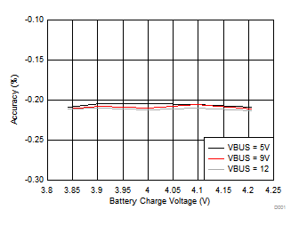
| VBAT(REG) |
Charge voltage resolution accuracy |
VBAT = 4.208 V (REG06[7:2] = 010111) or
VBAT = 4.352 V (REG06[7:2] = 100000)
TJ = -40°C - 85°C |
-0.5% |
|
0.5% |
|
| I(CHG_REG_RANGE) |
Typical fast charge current regulation range |
|
0 |
|
4032 |
mA |
| I(CHG_REG_STEP) |
Typical fast charge current regulation step |
|
|
64 |
|
mA |
| I(CHG_REG_ACC) |
Fast charge current regulation accuracy |
VBAT= 3.1 V or 3.8 V, ICHG = 256 mA
TJ = -40°C - 85°C |
-20% |
|
20% |
|
VBAT= 3.1 V or 3.8 V, ICHG = 1792 mA
TJ = -40°C - 85°C |
-5% |
|
5% |
|
| VBAT(LOWV) |
Battery LOWV falling threshold |
Fast charge to precharge, BATLOWV (REG06[1]) = 1 |
2.6 |
2.8 |
2.9 |
V |
| Battery LOWV rising threshold |
Precharge to fast charge, BATLOWV (REG06[1]) = 1
(Typical 200-mV hysteresis) |
2.8 |
3.0 |
3.15 |
V |
| Battery LOWV falling threshold |
Fast charge to precharge, BATLOWV (REG06[1]) = 0 |
2.5 |
2.6 |
2.7 |
V |
| Battery LOWV rising threshold |
Precharge to fast charge, BATLOWV (REG06[1]) = 0
(Typical 200-mV hysteresis) |
2.7 |
2.8 |
2.9 |
V |
| I(PRECHG_RANGE) |
Precharge current range |
|
64 |
|
1024 |
mA |
| I(PRECHG_STEP) |
Typical precharge current step |
|
|
64 |
|
mA |
| I(PRECHG_ACC) |
Precharge current accuracy |
VBAT = 2.6 V, IPRECHG = 256 mA |
–20% |
|
20% |
|
| I(TERM_RANGE) |
Termination current range |
|
64 |
|
1024 |
mA |
| I(TERM_STEP) |
Typical termination current step |
|
|
64 |
|
mA |
| I(TERM_ACC) |
Termination current accuracy |
ITERM = 256 mA, ICHG≤ 1344 mA
TJ = -20°C - 85°C |
-20% |
|
20% |
|
ITERM = 256 mA, ICHG> 1344 mA
TJ = -20°C - 85°C |
-20% |
|
20% |
|
| V(SHORT) |
Battery short voltage |
VBAT falling |
|
2.0 |
|
V |
| V(SHORT_HYST) |
Battery short voltage hysteresis |
VBAT rising |
|
200 |
|
mV |
| I(SHORT) |
Battery short current |
VBAT < 2.2 V |
|
110 |
|
mA |
| V(RECHG) |
Recharge threshold below VBATREG |
VBAT falling, VRECHG (REG06[0] = 0) = 0 |
|
100 |
|
mV |
| VBAT falling, VRECHG (REG06[0] = 0) = 1 |
|
200 |
|
mV |
| IBAT(LOAD) |
Battery discharge load current |
VBAT = 4.2 V |
15 |
|
|
mA |
| ISYS(LOAD) |
System discharge load current |
VSYS = 4.2 V |
30 |
|
|
mA |
| RON(BATFET) |
SYS-BAT MOSFET (BATFET) on-resistance |
TJ = 25°C |
|
5 |
7 |
mΩ |
| TJ = -40°C - 125°C |
|
5 |
10 |
mΩ |
| RBATSEN |
BATSEN input resistance |
|
|
800 |
|
kΩ |
| INPUT VOLTAGE / CURRENT REGULATION |
| VIN(DPM_RANGE) |
Typical input voltage regulation range |
|
3.9 |
|
15.3 |
V |
| VIN(DPM_STEP) |
Typical input voltage regulation step |
|
|
100 |
|
mV |
| VIN(DPM_ACC) |
Input voltage regulation accuracy |
VINDPM = 4.4 V, 7.8 V, 10.8 V |
-3% |
|
3% |
|
| IIN(DPM_RANGE) |
Typical input current regulation range |
|
100 |
|
3250 |
mA |
| IIN(DPM_STEP) |
Typical input current regulation step |
|
|
50 |
|
mA |
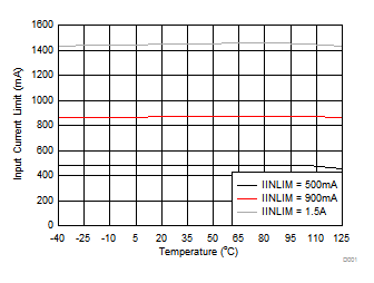
| IIN(DPM100_ACC) |
Input current 100mA regulation accuracy
VBAT = 5V, current pulled from SW |
IINLIM (REG00[5:0]) = 100 mA |
85 |
90 |
100 |
mA |
| IIN(DPM_ACC) |
Input current regulation accuracy
VBAT = 5V, current pulled from SW |
USB150, IINLIM (REG00[5:0]) = 150 mA |
125 |
135 |
150 |
mA |
| USB500, IINLIM (REG00[5:0]) = 500 mA |
440 |
470 |
500 |
mA |
| USB900, IINLIM (REG00[5:0]) = 900 mA |
750 |
825 |
900 |
mA |
| Adapter 1.5 A, IINLIM (REG00[5:0]) = 1500 mA |
1300 |
1400 |
1500 |
mA |
| IIN(START) |
Input current regulation during system start up |
VSYS = 2.2 V, IINLIM (REG00[5:0]) ≥ 200 mA |
|
|
200 |
mA |
| KILIM |
|
IINMAX = KILIM/RILIM, Input Current regulation by ILIM pin = 1.5 A |
290 |
320 |
350 |
A x Ω |
| VOK (bq25898)/DSEL (bq25898D) |
| VVOK_OH |
Voltage |
VBUS > 6 V I(VOK) = 20 mA and I(REGN) = 30 mA |
4.75 |
|
5.25 |
V |
| VBUS = 5 V I(VOK) = 5 mA and I(REGN) = 30 mA |
4.35 |
|
4.8 |
V |
| VVOK_OL |
Voltage |
Battery only VBAT = 3.8 V, I(VOK) = -10 mA |
|
|
0.4 |
V |
| VDSEL_OH |
Voltage |
I(DSEL) = 20 mA and I(REGN) = 30 mA, VBUS = 5 V |
1.3 |
|
|
V |
| VDSEL_OL |
Voltage |
I(DSEL) = -10 mA and I(REGN) = 30 mA, VBUS = 5 V |
|
|
0.4 |
V |
| D+/D- DETECTION (bq25898D) |
| I(10UA_ISRC) |
D+ connection check current source |
|
7 |
10 |
14 |
µA |
| I(100UA_ISINK) |
D+/D- current sink (100 µA) |
|
50 |
100 |
150 |
µA |
| I(DPDM_LKG) |
D+/D- Leakage current |
D–, switch open |
–1 |
|
1 |
µA |
| D+, switch open |
–1 |
|
1 |
µA |
| I(1P6MA_ISINK) |
D+/D- current sink (1.6 mA) |
|
1.35 |
1.60 |
1.75 |
mA |
| R(D–_DWN) |
D– pulldown for connection check |
|
14.25 |
|
24.8 |
kΩ |
| VFLOAT_VDPSRC |
D+/D- Voltage source (HIZ) |
REG01[7:5] = 000 (default) or REG01[4:2] = 000 (default) |
|
HIZ |
|
V |
| V0P0_VDSRC |
D+/D- Voltage source (0 V) |
REG01[7:5] = 001 or REG01[4:2] = 001 |
0 |
|
0.15 |
V |
| V0P6_VDSRC |
D+/D- Voltage source (0.6 V) |
REG01[7:5] = 010 or REG01[4:2] = 010 |
0.5 |
0.6 |
0.7 |
V |
| V1P2_DPVSRC |
D+/D- Voltage source (1.2 V) |
REG01[7:5] = 011 or REG01[4:2] = 011 |
1.075 |
1.2 |
1.325 |
V |
| V2P0_DPVSRC |
D+/D- Voltage source (2.0 V) |
REG01[7:5] = 100 or REG01[4:2] = 100 |
1.875 |
2 |
2.125 |
V |
| V2P7_DPVSRC |
D+/D- Voltage source (2.7 V) |
REG01[7:5] = 101 or REG01[4:2] = 101 |
2.575 |
2.7 |
2.825 |
V |
| V3P3_DPVSRC |
D+/D- Voltage source (3.3 V) |
REG01[7:5] = 110 or REG01[4:2] = 110 or REG01[4:2] = 111 |
3.15 |
3.3 |
3.45 |
V |
| RDPDM_SHORT |
D+/D- Short REG01[7:5] = 111 |
|
|
|
200 |
Ω |
| V(0P4_VTH) |
D+/D- low comparator threshold |
|
250 |
|
400 |
mV |
| V(0P8_VTH) |
D+ low comparator threshold |
|
|
|
0.8 |
V |
| V(2P7_VTH) |
D+/D- comparator threshold for non-standard adapter detection (Divider 1, 3,or 4) |
|
2.55 |
|
2.85 |
V |
| V(2P0_VTH) |
D+/D- comparator threshold for non-standard adapter detection (Divider 1, 3) |
|
1.85 |
|
2.15 |
V |
| V(1P2_VTH) |
D+/D- comparator threshold for non-standard adapter detection (Divider 2) |
|
1.05 |
|
1.35 |
V |
| BAT OVER-VOLTAGE/CURRENT PROTECTION |
| VBAT(OVP) |
Battery over-voltage threshold |
VBAT rising, as percentage of VBAT(REG) |
|
104% |
|
|
| VBAT(OVP_HYST) |
Battery over-voltage hysteresis |
VBAT falling, as percentage of VBAT(REG) |
|
2% |
|
|
| IBAT(FET_OCP) |
System over-current threshold |
|
9 |
|
|
A |
| THERMAL REGULATION AND THERMAL SHUTDOWN |
| TREG |
Junction temperature regulation accuracy |
REG08[1:0] = 11 |
|
120 |
|
°C |
| TSHUT |
Thermal shutdown rising temperature |
Temperature rising |
|
160 |
|
°C |
| TSHUT(HYS) |
Thermal shutdown hysteresis |
Temperature falling |
|
30 |
|
°C |
| JEITA THERMISTOR COMPARATOR (BUCK MODE) |
| V(T1) |
T1 (0°C) threshold, charge suspended T1 below this temperature. |
As percentage to V(REGN) |
72.75% |
73.25% |
73.75% |
|
| V(T1_HYS) |
Charge back to ICHG/2 (REG04[6:0]) and VREG (REG06[7:2]) above this temperature. |
As Percentage to V(REGN) |
|
1.4% |
|
|
| V(T2) |
T2 (10°C) threshold, charge back to ICHG/2 (REG04[6:0]) and VREG (REG06[7:2]) below this temperature. |
As Percentage to V(REGN) |
67.75% |
68.25% |
68.75% |
|
| V(T2_HYS) |
Charge back to ICHG (REG04[6:0]) and VREG (REG06[7:2]) above this temperature. |
As Percentage to V(REGN) |
|
1.4% |
|
|
| V(T3) |
T3 (45°C) threshold,charge back to ICHG (REG04[6:0]) and VREG-200mV (REG06[7:2]) above this temperature. |
As percentage to V(REGN) |
44.25v |
44.75% |
45.25% |
|
| V(T3_HYS) |
Charge back to ICHG (REG04[6:0]) and VREG (REG06[7:2]) below this temperature. |
As Percentage to V(REGN) |
|
1% |
|
|
| V(T5) |
T5 (60°C) threshold, charge suspended above this temperature. |
As Percentage to V(REGN) |
33.875% |
34.375% |
34.875% |
|
| V(T5_HYS) |
Charge back to ICHG (REG04[6:0]) and VREG-200mV (REG06[7:2]) below this temperature. |
As Percentage to V(REGN) |
|
1.25% |
|
|
| COLD/HOT THERMISTOR COMPARATOR (BOOST MODE) |
| V(BCOLD1) |
Cold temperature threshold 1, TS pin voltage rising threshold |
As percentage to VREGN REG01[5] = 1
(Approx. -20°C w/ 103AT) |
79.5% |
80% |
80.5% |
|
| V(BCOLD1_HYS) |
Cold temperature threshold 1, TS pin voltage falling threshold |
As percentage to VREGN REG01[5] = 1 |
|
1% |
|
|
| V(BHOT2) |
Hot temperature threshold 2, TS pin voltage falling threshold |
As percentage to VREGN REG01[7:6] = 10
(Approx. 65°C w/ 103AT) |
30.75% |
31.25% |
31.75% |
|
| V(BHOT2_HYS) |
Hot temperature threshold 2, TS pin voltage rising threshold |
As percentage to VREGN REG01[7:6] = 10 |
|
3% |
|
|
| PWM |
| FSW |
PWM switching frequency, and digital clock |
Oscillator frequency |
1.32 |
|
1.68 |
MHz |
| DMAX |
Maximum PWM duty cycle |
|
|
97% |
|
|
| BOOST MODE OPERATION |
| V(OTG_REG_RANGE) |
Typical boost mode regulation voltage range |
|
4.55 |
|
5.55 |
V |
| V(OTG_REG_STEP) |
Typical boost Mode Regulation voltage step |
|
|
64 |
|
mV |
| V(OTG_REG_ACC) |
Boost mode regulation voltage accuracy |
I(VBUS) = 0 A, BOOSTV = 4.998 V (REG0A[7:4] = 0111) |
-3% |
|
3% |
|
| V(OTG_BAT) |
Battery voltage exiting boost mode |
BAT falling, REG03[0] = 0 |
2.7 |
|
2.9 |
V |
| BAT falling, REG03[0] = 1 |
2.4 |
|
2.6 |
V |
| I(OTG) |
Typical boost mode output current range |
|
0.5 |
|
2.45 |
A |
| I(OTG_OCP_ACC) |
Boost mode RBFET over-current protection accuracy |
BOOST_LIM = 1.5 A (REG0A[2:0] = 100) |
1.5 |
|
2.0 |
A |
| V(OTG_OVP) |
Boost mode over-voltage threshold |
Rising threshold |
5.8 |
6 |
|
V |
| REGN LDO |
| V(REGN) |
REGN LDO output voltage |
V(VBUS) = 9 V, I(REGN) = 40 mA |
5.6 |
6 |
6.4 |
V |
| V(VBUS) = 5 V, I(REGN) = 20 mA |
4.7 |
4.8 |
|
V |
| I(REGN) |
REGN LDO current limit |
V(VBUS) = 9 V, V(REGN) = 3.8 V |
50 |
|
|
mA |
| ANALOG-TO-DIGITAL CONVERTER (ADC) |
| RES |
Resolution |
Rising threshold |
|
7 |
|
bits |
| VBAT(RANGE) |
Typical battery voltage range |
V(VBUS) > VBAT + V(SLEEP) or OTG mode is enabled |
2.304 |
|
4.848 |
V |
| V(VBUS) < VBAT + V(SLEEP) and OTG mode is disabled |
VSYS_MIN |
|
4.848 |
V |
| V(BAT_RES) |
Typical battery voltage resolution |
|
|
20 |
|
mV |
| V(SYS_RANGE) |
Typical system voltage range |
V(VBUS) > VBAT + V(SLEEP) or OTG mode is enabled |
2.304 |
|
4.848 |
V |
| V(VBUS) < VBAT + V(SLEEP) and OTG mode is disabled |
VSYS_MIN |
|
4.848 |
V |
| V(SYS_RES) |
Typical system voltage resolution |
|
|
20 |
|
mV |
| V(VBUS_RANGE) |
Typical VVBUS voltage range |
V(VBUS) > VBAT + V(SLEEP) or OTG mode is enabled |
2.6 |
|
15.3 |
V |
| V(VBUS_RES) |
Typical VVBUS voltage resolution |
|
|
100 |
|
mV |
| IBAT(RANGE) |
Typical battery charge current range |
V(VBUS) > VBAT + V(SLEEP) and VBAT > VBAT(SHORT) |
0 |
|
4.032 |
A |
| IBAT(RES) |
Typical battery charge current resolution |
|
|
50 |
|
mA |
| V(TS_RANGE) |
Typical TS voltage range |
|
21% |
|
80% |
|
| V(TS_RES) |
Typical TS voltage resolution |
|
|
0.47% |
|
|
| LOGIC I/O PIN (OTG, CE, PSEL, QON) |
| VIH |
Input high threshold level |
|
1.3 |
|
|
V |
| VIL |
Input low threshold level |
|
|
|
0.4 |
V |
| IIN(BIAS) |
High level leakage current |
Pull-up rail 1.8 V |
|
|
1 |
µA |
| V(QON) |
Internal /QON pull-up |
Battery only mode |
|
BAT |
|
V |
| V(VBUS) = 9 V |
|
5.8 |
|
V |
| V(VBUS) = 5 V |
|
4.3 |
|
V |
| R(QON) |
Internal /QON pull-up resistance |
|
|
200 |
|
kΩ |
| LOGIC I/O PIN (INT, STAT, PG) |
| VOL |
Output low threshold level |
Sink Current = 5 mA, Sink current |
|
|
0.4 |
V |
| IOUT_BIAS |
High level leakage current |
Pull-up rail 1.8 V |
|
|
1 |
µA |
| I2C INTERFACE (SCL, SDA) |
| VIH |
Input high threshold level, SCL and SDA |
Pull-up rail 1.8 V |
1.3 |
|
|
V |
| VIL |
Input low threshold level |
Pull-up rail 1.8 V |
|
|
0.4 |
V |
| VOL |
Output low threshold level |
Sink Current = 5 mA, Sink current |
|
|
0.4 |
V |
| IBIAS |
High level leakage current |
Pull-up rail 1.8 V |
|
|
1 |
µA |
