ZHCSD75D March 2014 – January 2018
PRODUCTION DATA.
- 1 特性
- 2 应用
- 3 说明
- 4 修订历史记录
- 5 Pin Configuration and Functions
-
6 Specifications
- 6.1 Absolute Maximum Ratings
- 6.2 ESD Ratings
- 6.3 Recommended Operating Conditions
- 6.4 Thermal Information
- 6.5 Power-On Reset
- 6.6 2.5-V LDO Regulator
- 6.7 Charger Attachment and Removal Detection
- 6.8 CHG and DSG FET Drive
- 6.9 Overvoltage Protection (OVP)
- 6.10 Undervoltage Protection (UVP)
- 6.11 Overcurrent in Discharge (OCD)
- 6.12 Overcurrent in Charge (OCC)
- 6.13 Short-Circuit in Discharge (SCD)
- 6.14 Low Voltage Charging
- 6.15 Internal Temperature Sensor Characteristics
- 6.16 High-Frequency Oscillator
- 6.17 Low-Frequency Oscillator
- 6.18 Integrating ADC (Coulomb Counter) Characteristics
- 6.19 ADC (Temperature and Cell Voltage) Characteristics
- 6.20 Data Flash Memory Characteristics
- 6.21 Timing Requirements
- 6.22 Typical Characteristics
-
7 Detailed Description
- 7.1 Overview
- 7.2 Functional Block Diagram
- 7.3 Feature Description
- 7.4 Device Functional Modes
- 7.5 Battery Parameter Measurements
- 7.6 Communications
- 7.7 Standard Data Commands
- 7.8 Extended Data Commands
-
8 Application and Implementation
- 8.1 Application Information
- 8.2
Typical Applications
- 8.2.1 Pack-Side, Single-Cell Li-Ion Fuel Gauge and Protector
- 8.2.2 Design Requirements
- 8.2.3
Detailed Design Procedure
- 8.2.3.1 BAT Voltage Sense Input
- 8.2.3.2 SRP and SRN Current Sense Inputs
- 8.2.3.3 Sense Resistor Selection
- 8.2.3.4 TS Temperature Sense Input
- 8.2.3.5 Thermistor Selection
- 8.2.3.6 VPWR Power Supply Input Filtering
- 8.2.3.7 REG25 LDO Output Filtering
- 8.2.3.8 Communication Interface Lines
- 8.2.3.9 PACKP Voltage Sense Input
- 8.2.3.10 CHG and DSG Charge Pump Voltage Outputs
- 8.2.3.11 NFET Selection
- 8.2.3.12 Additional ESD Protection Components
- 8.2.4 Application Curves
- 9 Power Supply Recommendation
- 10Layout
- 11器件和文档支持
- 12机械、封装和可订购信息
6.21 Timing Requirements
TA = –40°C to 85°C, 2.4 V < VREG25< 2.6 V; typical values at TA = 25°C and VREG25 = 2.5 V (unless otherwise noted)| MIN | NOM | MAX | UNIT | ||
|---|---|---|---|---|---|
| I2C-Compatible Interface Timing Characteristics (see Figure 1) | |||||
| tR | SCL or SDA rise time | 300 | ns | ||
| tF | SCL or SDA fall time | 300 | ns | ||
| tw(H) | SCL pulse width (high) | 600 | ns | ||
| tw(L) | SCL pulse width (low) | 1.3 | μs | ||
| tsu(STA) | Setup for repeated start | 600 | ns | ||
| td(STA) | Start to first falling edge of SCL | 600 | ns | ||
| tsu(DAT) | Data setup time | 100 | ns | ||
| th(DAT) | Data hold time | 0 | ns | ||
| tsu(STOP) | Setup time for stop | 600 | ns | ||
| tBUF | Bus free time between stop and start | 66 | μs | ||
| fSCL | Clock frequency | 400 | kHz | ||
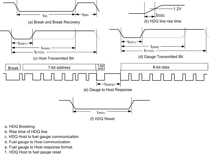
| HDQ Communication Timing Characteristics (see Figure 2) | |||||
| t(CYCH) | Cycle time, host to fuel gauge | 190 | μs | ||
| t(CYCD) | Cycle time, fuel gauge to host | 190 | 205 | 250 | μs |
| t(HW1) | Host sends 1 to fuel gauge | 0.5 | 50 | μs | |
| t(DW1) | Fuel gauge sends 1 to host | 32 | 50 | μs | |
| t(HW0) | Host sends 0 to fuel gauge | 86 | 145 | μs | |
| t(DW0) | Fuel gauge sends 0 to host | 80 | 145 | μs | |
| t(RSPS) | Response time, fuel gauge to host | 190 | 950 | μs | |
| t(B) | Break time | 190 | μs | ||
| t(BR) | Break recovery time | 40 | μs | ||
| t(RST) | HDQ reset | 1.8 | 2.2 | s | |
| t(RISE) | HDQ line rise time to logic 1 (1.2 V) | 950 | ns | ||
 Figure 1. I2C-Compatible Interface Timing Diagrams

a. HDQ Breaking
b. Rise time of HDQ line
c. HDQ Host to fuel gauge communication
d. Fuel gauge to Host communication
e. Fuel gauge to Host response format
f. HDQ Host to fuel gauge reset
Figure 2. HDQ Communication Timing Diagrams