ZHCSJJ2B March 2019 – December 2022 BQ27Z561-R1
PRODUCTION DATA
- 1 特性
- 2 应用
- 3 说明
- 4 Revision History
- 5 说明(续)
- 6 Pin Configuration and Functions
-
7 Specifications
- 7.1 Absolute Maximum Ratings
- 7.2 ESD Ratings
- 7.3 Recommended Operating Conditions
- 7.4 Thermal Information
- 7.5 Supply Current
- 7.6 Internal 1.8-V LDO (REG18)
- 7.7 I/O (PULS, INT)
- 7.8 Chip Enable (CE)
- 7.9 Internal Temperature Sensor
- 7.10 NTC Thermistor Measurement Support
- 7.11 Coulomb Counter (CC)
- 7.12 Analog Digital Converter (ADC)
- 7.13 Internal Oscillator Specifications
- 7.14 Voltage Reference1 (REF1)
- 7.15 Voltage Reference2 (REF2)
- 7.16 Flash Memory
- 7.17 I2C I/O
- 7.18 I2C Timing — 100 kHz
- 7.19 I2C Timing — 400 kHz
- 7.20 HDQ Timing
- 7.21 Typical Characteristics
-
8 Detailed Description
- 8.1 Overview
- 8.2 Functional Block Diagram
- 8.3
Feature Description
- 8.3.1 BQ27Z561-R1 Processor
- 8.3.2 Battery Parameter Measurements
- 8.3.3 Power Supply Control
- 8.3.4 Bus Communication Interface
- 8.3.5 Low Frequency Oscillator
- 8.3.6 High Frequency Oscillator
- 8.3.7 1.8-V Low Dropout Regulator
- 8.3.8 Internal Voltage References
- 8.3.9 Gas Gauging
- 8.3.10 Charge Control Features
- 8.3.11 Authentication
- 8.4 Device Functional Modes
- 9 Applications and Implementation
- 10Power Supply Requirements
- 11Layout
- 12Device and Documentation Support
- 13Mechanical, Packaging, Orderable Information
7.21 Typical Characteristics

A.
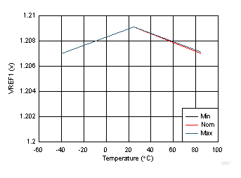
Figure 7-3 REF1 Voltage Versus Battery and Temperature| BAT Min = 2 V | BAT Nom = 3.6 V | BAT Max = 5 V |

A.
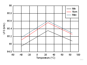
Figure 7-5 LFO Frequency Versus Battery and Temperature| BAT Min = 2 V | BAT Nom = 3.6 V | BAT Max = 5 V |

A.
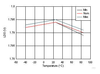
Figure 7-4 LDO Voltage Versus Battery and Temperature| BAT Min = 2 V | BAT Nom = 3.6 V | BAT Max = 5 V |

A.
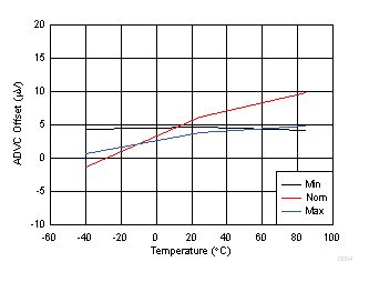
Figure 7-6 ADVC Offset Voltage Versus Battery and Temperature| BAT Min = 2 V | BAT Nom = 3.6 V | BAT Max = 5 V |