ZHCSKS9B February 2020 – November 2022 BQ27Z561-R2
PRODUCTION DATA
- 1 特性
- 2 应用
- 3 说明
- 4 Revision History
- 5 说明(续)
- 6 Pin Configuration and Functions
-
7 Specifications
- 7.1 Absolute Maximum Ratings
- 7.2 ESD Ratings
- 7.3 Recommended Operating Conditions
- 7.4 Thermal Information
- 7.5 Supply Current
- 7.6 Internal 1.8-V LDO (REG18)
- 7.7 I/O (PULS, INT)
- 7.8 Chip Enable (CE)
- 7.9 Internal Temperature Sensor
- 7.10 NTC Thermistor Measurement Support
- 7.11 Coulomb Counter (CC)
- 7.12 Analog Digital Converter (ADC)
- 7.13 Internal Oscillator Specifications
- 7.14 Voltage Reference1 (REF1)
- 7.15 Voltage Reference2 (REF2)
- 7.16 Flash Memory
- 7.17 I2C I/O
- 7.18 I2C Timing — 100 kHz
- 7.19 I2C Timing — 400 kHz
- 7.20 HDQ Timing
- 7.21 Typical Characteristics
-
8 Detailed Description
- 8.1 Overview
- 8.2 Functional Block Diagram
- 8.3
Feature Description
- 8.3.1 BQ27Z561-R2 Processor
- 8.3.2 Battery Parameter Measurements
- 8.3.3 Power Supply Control
- 8.3.4 Bus Communication Interface
- 8.3.5 Low Frequency Oscillator
- 8.3.6 High Frequency Oscillator
- 8.3.7 1.8-V Low Dropout Regulator
- 8.3.8 Internal Voltage References
- 8.3.9 Gas Gauging
- 8.3.10 Charge Control Features
- 8.3.11 Authentication
- 8.4 Device Functional Modes
- 9 Applications and Implementation
- 10Device and Documentation Support
- 11Mechanical, Packaging, and Orderable Information
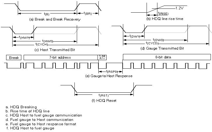
7.20 HDQ Timing
| PARAMETER | TEST CONDITIONS | MIN | NOM | MAX | UNIT | |
|---|---|---|---|---|---|---|
| tB | Break time | 190 | µs | |||
| tBR | Break recovery time | 40 | µs | |||
| tHW1 | Host write 1 time | Host drives HDQ | 0.5 | 50 | µs | |
| tHW0 | Host write 0 time | Host drives HDQ | 86 | 145 | µs | |
| tCYCH | Cycle time, host to device | Device drives HDQ | 190 | µs | ||
| tCYCD | Cycle time, device to Host | Device drives HDQ | 190 | 205 | 250 | µs |
| tDW1 | Device write 1 time | Device drives HDQ | 32 | 50 | µs | |
| tDW0 | Device write 0 time | Device drives HDQ | 80 | 145 | µs | |
| tRSPS | Device response time | Device drives HDQ | 190 | 950 | µs | |
| tTRND | Host turn around time | Host drives HDQ after device drives HDQ | 250 | µs | ||
| tRISE | HDQ line rising time to logic 1 | 1.8 | µs | |||
| tRST | HDQ Reset | Host drives HDQ low before device reset | 2.2 | s | ||
 Figure 7-1 I2C Timing
 Figure 7-2 HDQ Timing