SLUSFQ0 November 2024 BQ27Z758
PRODUCTION DATA
- 1
- 1 Features
- 2 Applications
- 3 Description
- 4 Pin Configurations and Functions
- 5 Specifications
-
6 Detailed Description
- 6.1 Overview
- 6.2 Functional Block Diagram
- 6.3
Feature Description
- 6.3.1 BQ27Z758 Processor
- 6.3.2 Battery Parameter Measurements
- 6.3.3 Power Supply Control
- 6.3.4 ENAB Pin
- 6.3.5 Bus Communication Interface
- 6.3.6 Low Frequency Oscillator
- 6.3.7 High Frequency Oscillator
- 6.3.8 1.8-V Low Dropout Regulator
- 6.3.9 Internal Voltage References
- 6.3.10 Overcurrent in Discharge Protection
- 6.3.11 Overcurrent in Charge Protection
- 6.3.12 Short-Circuit Current in Discharge Protection
- 6.3.13 Primary Protection Features
- 6.3.14 Battery Sensing
- 6.3.15 Gas Gauging
- 6.3.16 Zero Volt Charging (ZVCHG)
- 6.3.17 Charge Control Features
- 6.3.18 Authentication
- 6.4 Device Functional Modes
- 7 Applications and Implementation
- 8 Power Supply Requirements
- 9 Layout
- 10Device and Documentation Support
- 11Revision History
- 12Mechanical, Orderable, and Packaging Information
5.7 Digital I/O: Timing Characteristics
| PARAMETER | TEST CONDITIONS | MIN | NOM | MAX | UNIT | |
|---|---|---|---|---|---|---|
| I2C Timing — 100 kHz | ||||||
| fSCL | Clock Operating Frequency | SCL duty cycle = 50% | 100 | kHz | ||
| tHD:STA | START Condition Hold Time | 4.0 | µs | |||
| tLOW | Low period of the SCL Clock | 4.7 | µs | |||
| tHIGH | High period of the SCL Clock | 4.0 | µs | |||
| tSU:STA | Setup repeated START | 4.7 | µs | |||
| tHD:DAT | Data hold time (SDA input) | 0 | ns | |||
| tSU:DAT | Data setup time (SDA input) | 250 | ns | |||
| tr | Clock Rise Time | 10% to 90% | 1000 | ns | ||
| tf | Clock Fall Time | 90% to 10% | 300 | ns | ||
| tSU:STO | Setup time STOP Condition | 4.0 | µs | |||
| tBUF | Bus free time STOP to START | 4.7 | µs | |||
| I2C Timing — 400 kHz | ||||||
| fSCL | Clock Operating Frequency | SCL duty cycle = 50% | 400 | kHz | ||
| tHD:STA | START Condition Hold Time | 0.6 | µs | |||
| tLOW | Low period of the SCL Clock | 1.3 | µs | |||
| tHIGH | High period of the SCL Clock | 600 | ns | |||
| tSU:STA | Setup repeated START | 600 | ns | |||
| tHD:DAT | Data hold time (SDA input) | 0 | ns | |||
| tSU:DAT | Data setup time (SDA input) | 100 | ns | |||
| tr | Clock Rise Time | 10% to 90% | 300 | ns | ||
| tf | Clock Fall Time | 90% to 10% | 300 | ns | ||
| tSU:STO | Setup time STOP Condition | 0.6 | µs | |||
| tBUF | Bus free time STOP to START | 1.3 | µs | |||
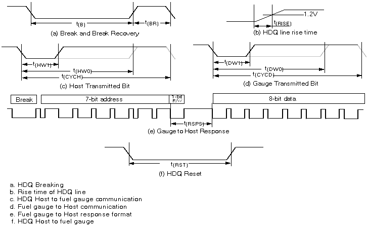
| HDQ Timing | ||||||
| tB | Break Time | 190 | µs | |||
| tBR | Break Recovery Time | 40 | µs | |||
| tHW1 | Host Write 1 Time | Host drives HDQ | 0.5 | 50 | µs | |
| tHW0 | Host Write 0 Time | Host drives HDQ | 86 | 145 | µs | |
| tCYCH | Cycle Time, Host to device | device drives HDQ | 190 | µs | ||
| tCYCD | Cycle Time, device to Host | device drives HDQ | 190 | 205 | 250 | µs |
| tDW1 | Device Write 1 Time | device drives HDQ | 32 | 50 | µs | |
| tDW0 | Device Write 0 Time | device drives HDQ | 80 | 145 | µs | |
| tRSPS | Device Response Time | device drives HDQ | 190 | 950 | µs | |
| tTRND | Host Turn Around Time | Host drives HDQ after device drives HDQ | 250 | µs | ||
| tRISE | HDQ Line Rising Time to Logic 1 | 1.8 | µs | |||
| tRST | HDQ Reset | Host drives HDQ low before device reset | 2.2 | s | ||
 Figure 5-1 I2C Timing
 Figure 5-2 HDQ Timing