ZHCSDT5C September   2010  – March 2016

PRODUCTION DATA.  

  1. 特性
  2. 应用
  3. 说明
  4. 修订历史记录
  5. Device Options
  6. Pin Configuration and Functions
  7. Specifications
    1. 7.1 Absolute Maximum Ratings
    2. 7.2 ESD Ratings
    3. 7.3 Recommended Operating Conditions
    4. 7.4 Thermal Information
    5. 7.5 Electrical Characteristics
    6. 7.6 Recommended Cell Balancing Configurations
    7. 7.7 Typical Characteristics
  8. Detailed Description
    1. 8.1 Overview
      1. 8.1.1 Voltage Protection
      2. 8.1.2 Cell Balancing
    2. 8.2 Functional Block Diagram
    3. 8.3 Feature Description
      1. 8.3.1 Protection (OUT) Timing
      2. 8.3.2 Cell Voltage > VPROTECT
      3. 8.3.3 Cell Connection Sequence
      4. 8.3.4 Cell Balance Enable Control
      5. 8.3.5 Cell Balance Configuration
      6. 8.3.6 Cell Imbalance Auto-Detection (Via Cell Voltage)
      7. 8.3.7 Customer Test Mode
      8. 8.3.8 Test Conditions
    4. 8.4 Device Functional Modes
      1. 8.4.1 NORMAL Mode
      2. 8.4.2 PROTECTION Mode
  9. Application and Implementation
    1. 9.1 Application Information
    2. 9.2 Typical Applications
      1. 9.2.1 Battery Connection
        1. 9.2.1.1 Design Requirements
        2. 9.2.1.2 Detailed Design Procedure
        3. 9.2.1.3 Application Curve
    3. 9.3 System Example
      1. 9.3.1 External Cell Balancing
  10. 10Power Supply Recommendations
  11. 11Layout
    1. 11.1 Layout Guidelines
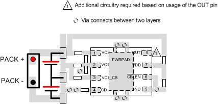
    2. 11.2 Layout Example
  12. 12器件和文档支持
    1. 12.1 相关链接
    2. 12.2 社区资源
    3. 12.3 商标
    4. 12.4 静电放电警告
    5. 12.5 Glossary
  13. 13机械、封装和可订购信息

封装选项

请参考 PDF 数据表获取器件具体的封装图。

机械数据 (封装 | 引脚)
  • DRB|8
散热焊盘机械数据 (封装 | 引脚)
订购信息

Layout

Layout Guidelines

The following are the recommended layout guidelines:

  1. Ensure the input filters to the VC1 and VC2 pins are as close to the IC as possible to improve noise immunity.
  2. If the OUT pin is used to control a high current path, for example: to blow a chemical fuse, then care should be taken to ensure the high current path creates minimal interference of the bq2920x voltage sense inputs.
  3. The input RC filter on the VDD pin should be close to the terminal of the IC.

Layout Example

bq29200 bq29209 layout_lusa52.gif