ZHCSDT5C September 2010 – March 2016
PRODUCTION DATA.
- 1 特性
- 2 应用
- 3 说明
- 4 修订历史记录
- 5 Device Options
- 6 Pin Configuration and Functions
- 7 Specifications
- 8 Detailed Description
- 9 Application and Implementation
- 10Power Supply Recommendations
- 11Layout
- 12器件和文档支持
- 13机械、封装和可订购信息
封装选项
请参考 PDF 数据表获取器件具体的封装图。
机械数据 (封装 | 引脚)
- DRB|8
散热焊盘机械数据 (封装 | 引脚)
- DRB|8
订购信息
7 Specifications
7.1 Absolute Maximum Ratings
Over-operating free-air temperature range (unless otherwise noted)(1)| MIN | MAX | UNIT | ||
|---|---|---|---|---|
| Supply voltage range, VMAX | VDD–GND | –0.3 | 16 | V |
| Input voltage range, VIN | VC2–GND, VC1–GND | –0.3 | 16 | V |
| VC2–VC1, CD–GND | –0.3 | 8 | V | |
| CB_EN–GND | –0.3 | 16 | V | |
| Output voltage range, VOUT | OUT–GND | –0.3 | 16 | V |
| Continuous total power dissipation, PTOT | See Thermal Information. | |||
| Storage temperature range, Tstg | –65 | 150 | °C | |
(1) Stresses beyond those listed under Absolute Maximum Ratings may cause permanent damage to the device. These are stress ratings only, which do not imply functional operation of the device at these or any other conditions beyond those indicated under Recommended Operating Conditions. Exposure to absolute-maximum-rated conditions for extended periods may affect device reliability.
7.2 ESD Ratings
| VALUE | UNIT | |||
|---|---|---|---|---|
| V(ESD) | Electrostatic discharge | Human-body model (HBM), per ANSI/ESDA/JEDEC JS-001(1) | ±2000 | V |
| Charged-device model (CDM), per JEDEC specification JESD22-C101(2) | ±500 | |||
(1) JEDEC document JEP155 states that 500-V HBM allows safe manufacturing with a standard ESD control process. Manufacturing with less than 500-V HBM is possible with the necessary precautions.
(2) JEDEC document JEP157 states that 250-V CDM allows safe manufacturing with a standard ESD control process. Manufacturing with less than 250-V CDM is possible with the necessary precautions.
7.3 Recommended Operating Conditions
| MIN | NOM | MAX | UNIT | ||
|---|---|---|---|---|---|
| Supply voltage, VDD | 4 | 10 | V | ||
| Input voltage range | VC2–VC1, VC1–GND | 0 | 5 | V | |
| Delay time capacitance, td(CD) | CCD (See Figure 9.) | 0.1 | µF | ||
| Voltage monitor filter resistance | RIN (See Figure 9.) | 100 | 1K | Ω | |
| Voltage monitor filter capacitance | CIN (See Figure 9.) | 0.01 | 0.1 | µF | |
| Supply voltage filter resistance | RVD (See Figure 9.) | 100 | 1K | Ω | |
| Supply voltage filter capacitance | CVD (See Figure 9.) | 0.1 | µF | ||
| Cell balance resistance | RCB (See Figure 9 and Protection (OUT) Timing.) | 100 | 4.7K | Ω | |
| Operating ambient temperature range, TA | –40 | 110 | °C | ||
7.4 Thermal Information
| THERMAL METRIC(1) | bq2920x | UNIT | |
|---|---|---|---|
| DRB | |||
| 8 PINS | |||
| RθJA | Junction-to-ambient thermal resistance | 50.5 | °C/W |
| RθJC(top) | Junction-to-case(top) thermal resistance | 25.1 | °C/W |
| RθJB | Junction-to-board thermal resistance | 19.3 | °C/W |
| ψJT | Junction-to-top characterization parameter | 0.7 | °C/W |
| ψJB | Junction-to-board characterization parameter | 18.9 | °C/W |
| RθJC(bot) | Junction-to-case(bottom) thermal resistance | 5.2 | °C/W |
(1) For more information about traditional and new thermal metrics, see the Semiconductor and IC Package Thermal Metrics application report, SPRA953.
7.5 Electrical Characteristics
Typical values stated where TA = 25°C and VDD = 7.2 V. Minimum and maximum values stated where TA = –40°C to 110°C and VDD = 4 V to 10 V (unless otherwise noted).| PARAMETER | TEST CONDITIONS | MIN | TYP | MAX | UNIT | ||
|---|---|---|---|---|---|---|---|
| VPROTECT | Overvoltage detection voltage | bq29209 | 4.3 | V | |||
| bq29200 | 4.35 | ||||||
| VHYS | Overvoltage detection hysteresis | 200 | 300 | 400 | mV | ||
| VOA | Overvoltage detection accuracy | TA = 25°C | –10 | 10 | mV | ||
| VOA_DRIFT | Overvoltage threshold temperature drift | TA = 0°C to 60°C | –0.4 | 0.4 | mV°/C | ||
| TA = –40°C to 110°C | –0.6 | 0.6 | |||||
| XDELAY | Overvoltage delay time scale factor | TA = 0°C to 60°C Note: Does not include external capacitor variation. |
6 | 9 | 12 | s/µF | |
| TA = –40°C to 110°C Note: Does not include external capacitor variation. |
5.5 | 9 | 13.5 | ||||
| XDELAY_CTM(1) | Overvoltage delay time scale factor in Customer Test Mode | 0.08 | s/µF | ||||
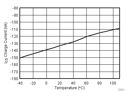
| ICD(CHG) | Overvoltage detection charging current | 150 | nA | ||||
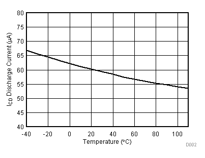
| ICD(DSG) | Overvoltage detection discharging current | 60 | µA | ||||
| VCD | Overvoltage detection external capacitor comparator threshold | 1.2 | V | ||||
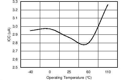
| ICC | Supply current | (VC2–VC1) = (VC1–GND) = 3.5 V (See Figure 7.) | 3 | 6 | µA | ||
| VOUT | OUT pin drive voltage | (VC2–VC1) or (VC1–GND) > VPROTECT, VDD = 10 V, IOH = 0 |
6 | 8.25 | 9.5 | V | |
| (VC2–VC1) or (VC1–GND) = VPROTECT, VDD = VPROTECT, IOH = –100 µA, TA = 0°C to 60°C |
1.75 | 2.5 | V | ||||
| (VC2–VC1) and (VC1–GND) < VPROTECT , IOL = 100 µA, TA = 25°C |
200 | mV | |||||
| (VC2–VC1) and (VC1–GND) < VPROTECT , IOL = 0 µA, TA = 25°C |
0 | 10 | mV | ||||
| VC2 = VC1 = VDD = 4 V, IOL = 100 µA | 200 | mV | |||||
| IOH | High-level output current | OUT = 1.75 V, (VC2–VC1) or (VC1–GND) = VPROTECT, VDD = VPROTECT to 10 V, TA = 0°C to 60°C | –100 | µA | |||
| IOL | Low-level output current | OUT = 0.05 V, (VC2–VC1) or (VC1–GND) < VPROTECT, VDD = VPROTECT to 10 V, TA = 0°C to 60°C | 30 | 85 | µA | ||
| IOH_ZV | High-level short-circuit output current | OUT = 0 V, (VC2–VC1) = (VC1–GND) = VPROTECT
VDD = 4 to 10 V |
–8 | mA | |||
| IIN | Input current at VCx pins | Measured at VC1, (VC2–VC1) = (VC1–GND) = 3.5 V, TA = 0°C to 60°C (See Figure 7.) |
–0.2 | 0.2 | µA | ||
| Measured at VC2, (VC2–VC1) = (VC1–GND) = 3.5 V, TA = 0°C to 60°C (See Figure 7.) |
2.5 | µA | |||||
| VMM_DET_ON | Cell mismatch detection threshold for turning ON | (VC2–VC1) versus (VC1–GND) and vice-versa when cell balancing is enabled. VC2 = VDD = 7.6 V | 17 | 30 | 45 | mV | |
| VMM_DET_OFF | Cell mismatch detection threshold for turning OFF | Delta between (VC2–VC1) and (VC1–GND) when cell balancing is disabled. VC2 = VDD = 7.6 V | –9 | 0 | 9 | mV | |
| VCB_EN_ON | Cell balance enable ON threshold | Active LOW pin at CB_EN | 1 | V | |||
| VCB_EN_OFF | Cell balance enable OFF threshold | Active HIGH at CB_EN | 2.2 | V | |||
| ICB_EN | Cell balance enable ON input current | CB_EN = GND (See Figure 8.) | 0.2 | µA | |||
| RCB1 | Internal cell balance switch resistance | CB_EN = GND | Ω | ||||
| RCB2 | Internal cell balance switch resistance | CB_EN = GND | Ω | ||||
(1) Specified by design. Not 100% tested in production.
7.6 Recommended Cell Balancing Configurations
Typical values stated where TA = 25°C and (VC2–VC1), (VC1–GND) = 3.8 V. Minimum and maximum values stated where TA = –40°C to 110°C, VDD = 4 V to 10 V, and (VC2–VC1), (VC1–GND) = 3 V to 4.2 V. All values assume recommended supply voltage filter resistance RVD of 100 Ω and 5% accurate or better cell balance resistor RCB.| MIN | NOM | MAX | UNIT | |||
|---|---|---|---|---|---|---|
| ICB | Cell balance input current | RCB = 4700 Ω | 0.5 | 0.75 | 1 | mA |
| RCB = 2200 Ω | 1 | 1.5 | 2 | |||
| RCB = 910 Ω | 2 | 3 | 4 | |||
| RCB = 560 Ω | 3 | 4.5 | 6 | |||
| RCB = 360 Ω | 3.5 | 6 | 8.5 | |||
| RCB = 240 Ω | 4 | 7.5 | 11 | |||
| RCB = 120 Ω | 5 | 10 | 15 | |||


