ZHCSHD3K October 2017 – July 2024 BQ2980 , BQ2982
PRODUCTION DATA
- 1
- 1 特性
- 2 应用
- 3 说明
- 4 Device Comparison Table
- 5 Pin Configuration and Functions
- 6 Specifications
-
7 Detailed Description
- 7.1 Overview
- 7.2 Functional Block Diagram
- 7.3
Feature Description
- 7.3.1 Overvoltage (OV) Status
- 7.3.2 Undervoltage (UV) Status
- 7.3.3 Overcurrent in Charge (OCC) Status
- 7.3.4 Overcurrent in Discharge (OCD) and Short Circuit in Discharge (SCD) Status
- 7.3.5 Overtemperature (OT) Status
- 7.3.6 Charge and Discharge Driver
- 7.3.7 CTR for FET Override and Device Shutdown
- 7.3.8 CTR for PTC Connection
- 7.3.9 ZVCHG (0-V Charging)
- 7.4 Device Functional Modes
- 8 Application and Implementation
- 9 Power Supply Recommendations
- 10Layout
- 11Device and Documentation Support
- 12Revision History
- 13Mechanical, Packaging, and Orderable Information
8.2.1.3 Selection of Power FET
The high-side driver of the BQ298x device limits the Vgs below 8 V with a 4.4-V battery cell. This means the device can work with a power FET with an absolute maximum rating as low as ±8 V Vgs, which is common in smartphone applications.
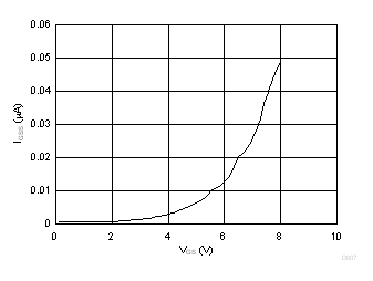
Additionally, TI highly recommends using a low gate leakage FET around 6-V to 7-V Vgs range. The power FET on the BQ298x evaluation module has the following typical gate leakage. TI recommends selecting a similar gate leakage FET for the design.
 Figure 8-7 Power FET (on BQ2980 EVM) Gate Leakage Versus Vgs