ZHCS692C October 2010 – October 2015
PRODUCTION DATA.
- 1 特性
- 2 应用
- 3 说明
- 4 修订历史记录
- 5 Pin Configuration and Functions
-
6 Specifications
- 6.1 Absolute Maximum Ratings
- 6.2 ESD Ratings
- 6.3 Recommended Operating Conditions
- 6.4 Thermal Information
- 6.5 Electrical Characteristics: Supply Current
- 6.6 Power-On Reset (POR)
- 6.7 Wake From Sleep
- 6.8 RBI RAM Backup
- 6.9 3.3-V Regulator
- 6.10 2.5-V Regulator
- 6.11 PRES, SMBD, SMBC
- 6.12 CHG, DSG FET Drive
- 6.13 PCHG FET Drive
- 6.14 FUSE
- 6.15 Coulomb Counter
- 6.16 VC1, VC2, VC3, VC4
- 6.17 TS1, TS2
- 6.18 Internal Temperature Sensor
- 6.19 Internal Thermal Shutdown
- 6.20 High-Frequency Oscillator
- 6.21 Low-Frequency Oscillator
- 6.22 Internal Voltage Reference
- 6.23 Flash
- 6.24 OCD Current Protection
- 6.25 SCD1 Current Protection
- 6.26 SCD2 Current Protection
- 6.27 SCC Current Protection
- 6.28 SBS Timing Requirements
- 6.29 Typical Characteristics
- 7 Parameter Measurement Information
- 8 Detailed Description
- 9 Application and Implementation
- 10Power Supply Recommendations
- 11Layout
- 12器件和文档支持
- 13机械、封装和可订购信息
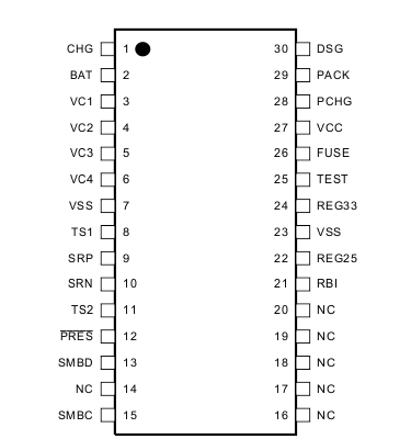
5 Pin Configuration and Functions
DBT Package
30-Pin TSSOP
Top View

Pin Functions
| PIN | TYPE(1) | DESCRIPTION | |
|---|---|---|---|
| NAME | NO. | ||
| BAT | 2 | P | Alternate power source |
| CHG | 1 | O | Charge N-FET gate drive |
| DSG | 30 | O | Discharge N-FET gate drive |
| FUSE | 26 | O | Fuse drive |
| NC | 14 | — | Not internally connected. Connect to VSS. |
| NC | 16 | — | Not internally connected. Connect to VSS. |
| NC | 17 | — | Not internally connected. Connect to VSS. |
| NC | 18 | — | Not internally connected. Connect to VSS. |
| NC | 19 | — | Not internally connected. Connect to VSS. |
| NC | 20 | — | Not internally connected. Connect to VSS. |
| PACK | 29 | P | Alternate power source |
| PCHG | 28 | I/OD | Precharge P-FET gate drive |
| PRES | 12 | I | Host system present input |
| RBI | 21 | P | RAM backup |
| REG25 | 22 | P | 2.5-V regulator output |
| REG33 | 24 | P | 3.3-V regulator output |
| SMBC | 15 | I/OD | SMBus v1.1 clock line |
| SMBD | 13 | I/OD | SMBus v1.1 data line |
| SRN | 10 | AI | Differential Coulomb Counter input |
| SRP | 9 | AI | Differential Coulomb Counter input |
| TEST | 25 | — | Test pin, connect to VSS through 2-kΩ resistor. |
| TS1 | 8 | AI | Temperature sensor 1 thermistor input |
| TS2 | 11 | AI | Temperature sensor 2 thermistor input |
| VC1 | 3 | I | Sense input for positive voltage of top most cell in stack and cell balancing input for top most cell in stack |
| VC2 | 4 | I | Sense input for positive voltage of third lowest cell in stack and cell balancing input for third lowest cell in stack |
| VC3 | 5 | I | Sense input for positive voltage of second lowest cell in stack and cell balancing input for second lowest cell in stack |
| VC4 | 6 | I | Sense input for positive voltage of lowest cell in stack and cell balancing input for lowest cell in stack |
| VCC | 27 | P | Power supply voltage |
| VSS | 7 | P | Device ground |
| VSS | 23 | P | Device ground |
(1) P = Power Connection, O = Digital Output, AI = Analog Input, I = Digital Input, I/OD = Digital Input/Output