SLUS900E December 2008 – August 2015
PRODUCTION DATA.
- 1 Features
- 2 Applications
- 3 Description
- 4 Revision History
- 5 Pin Configuration and Functions
- 6 Specifications
-
7 Detailed Description
- 7.1 Overview
- 7.2 Functional Block Diagram
- 7.3 Feature Description
- 7.4 Device Functional Modes
- 7.5 Programming
- 7.6
Register Maps
- 7.6.1 I2C Read After Backup Mode
- 7.6.2
Normal Register Descriptions
- 7.6.2.1 SECONDS Register (address = 0x00) [reset = 0XXXXXXb]
- 7.6.2.2 MINUTES Register (address = 0x01) [reset = 1XXXXXXb]
- 7.6.2.3 CENT_HOURS Register (address = 0x02) [reset = XXXXXXXXb]
- 7.6.2.4 DAY Register (address = 0x03) [reset = 00000XXXb]
- 7.6.2.5 DATE Register (address = 0x04) [reset = 00XXXXXXb]
- 7.6.2.6 MONTH Register (address = 0x05) [reset = 000XXXXXb]
- 7.6.2.7 YEARS Register (address = 0x06) [reset = XXXXXXXXb]
- 7.6.2.8 CAL_CFG1 Register (address = 0x07) [reset = 10000000b]
- 7.6.2.9 TCH2 Register (address = 0x08) [reset = 10010000b]
- 7.6.2.10 CFG2 Register (address = 0x09) [reset = 10101010b]
- 7.6.3 Special Function Registers
- 8 Application and Implementation
- 9 Power Supply Recommendations
- 10Layout
- 11Device and Documentation Support
- 12Mechanical, Packaging, and Orderable Information
10 Layout
10.1 Layout Guidelines
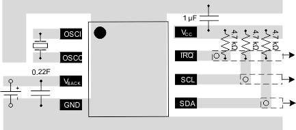
The VCC pin should be bypassed to GND using a low-ESR ceramic bypass capacitor with a minimum recommended value of 1-µF. This capacitor should be placed as close to the VCC and GND pins as possible with thick trace or ground plane connection to the device GND pin.
Locate the 32.768-kHz crystal oscillator as close as possible to the OSCI and OSCO pins. This will minimize stray capacitance.
10.2 Layout Example
 Figure 25. Recommended PCB Layout