ZHCSGI9 August 2017
PRODUCTION DATA.
- 1 特性
- 2 应用
- 3 说明
- 4 修订历史记录
- 5 Pin Configuration and Functions
-
6 Specifications
- 6.1 Absolute Maximum Ratings
- 6.2 ESD Ratings
- 6.3 Recommended Operating Conditions
- 6.4 Thermal Information
- 6.5 Supply Current
- 6.6 Digital Input and Output DC Characteristics
- 6.7 LDO Regulator, Wake-up, and Auto-Shutdown DC Characteristics
- 6.8 LDO Regulator, Wake-up, and Auto-Shutdown AC Characteristics
- 6.9 ADC (Temperature and Cell Measurement) Characteristics
- 6.10 Integrating ADC (Coulomb Counter) Characteristics
- 6.11 I2C-Compatible Interface Communication Timing
- 6.12 SHUTDOWN and WAKE-UP Timing
- 6.13 Typical Characteristics
-
7 Detailed Description
- 7.1 Overview
- 7.2 Functional Block Diagram
- 7.3
Feature Description
- 7.3.1 Device Configuration
- 7.3.2 ALERT Interrupt and SHUTDOWN Wake-up
- 7.3.3 Voltage Measurement and Calibration
- 7.3.4 Temperature Measurement
- 7.3.5 Charging and Termination
- 7.3.6 Accumulated Charge Measurement
- 7.3.7 Gas Gauging
- 7.3.8 Battery Condition Warnings
- 7.3.9 Configuration Update
- 7.3.10 End-Of-Service Determination
- 7.3.11 Battery Level Threshold
- 7.3.12 Communications
- 7.3.13 Additional Data Memory Parameter Descriptions
- 7.4 Device Functional Modes
- 8 Application and Implementation
- 9 Power Supply Recommendation
- 10Layout
- 11器件和文档支持
- 12机械、封装和可订购信息
10 Layout
10.1 Layout Guidelines
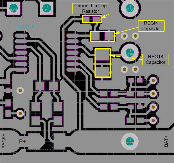
- A capacitor of a value of at least 2.2 µF is connected between the REG18 pin and VSS. The capacitor should be placed close to the fuel gauge and have short traces to both the REG18 pin and VSS as shown in bq34210-Q1 Capacitor Layout. This regulator must not be used to provide power for other devices in the system.
- If the connection between the battery pack and the gauge REGIN pin has the potential to pick up noise, it is required to have a capacitor of at least 1.0 µF connect between the REGIN pin and VSS. Place the capacitor close to the fuel gauge and have short traces to both the REGIN pin and VSS.
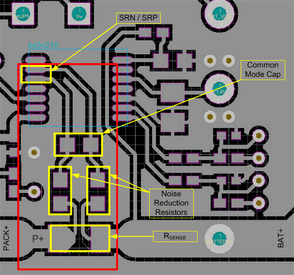
- The SRP and SRN pins should be Kelvin connected to the RSENSE terminals.
- For the low-side sense resistor:
- Connect SRP to the battery pack side of RSENSE and SRN to the system side of the RSENSE, as shown in bq34210-Q1 Sense Resistor Layout.
- Kelvin connect the REGIN pin to the battery PACK+ terminal.
10.2 Layout Example
 Figure 8. bq34210-Q1 Sense Resistor Layout
 Figure 9. bq34210-Q1 Capacitor Layout