ZHCSGX4C June 2017 – April 2021 BQ40Z50-R2
PRODUCTION DATA
- 1 特性
- 2 应用
- 3 说明
- 4 Revision History
- 5 Description (continued)
- 6 Pin Configuration and Functions
-
7 Specifications
- 7.1 Absolute Maximum Ratings
- 7.2 ESD Ratings
- 7.3 Recommended Operating Conditions
- 7.4 Thermal Information
- 7.5 Supply Current
- 7.6 Power Supply Control
- 7.7 AFE Power-On Reset
- 7.8 AFE Watchdog Reset and Wake Timer
- 7.9 Current Wake Comparator
- 7.10 VC1, VC2, VC3, VC4, BAT, PACK
- 7.11 SMBD, SMBC
- 7.12 PRES, BTP_INT, DISP
- 7.13 LEDCNTLA, LEDCNTLB, LEDCNTLC
- 7.14 Coulomb Counter
- 7.15 CC Digital Filter
- 7.16 ADC
- 7.17 ADC Digital Filter
- 7.18 CHG, DSG FET Drive
- 7.19 PCHG FET Drive
- 7.20 FUSE Drive
- 7.21 Internal Temperature Sensor
- 7.22 TS1, TS2, TS3, TS4
- 7.23 PTC, PTCEN
- 7.24 Internal 1.8-V LDO
- 7.25 High-Frequency Oscillator
- 7.26 Low-Frequency Oscillator
- 7.27 Voltage Reference 1
- 7.28 Voltage Reference 2
- 7.29 Instruction Flash
- 7.30 Data Flash
- 7.31 OLD, SCC, SCD1, SCD2 Current Protection Thresholds
- 7.32 Timing Requirements: OLD, SCC, SCD1, SCD2 Current Protection Timing
- 7.33 Timing Requirements: SMBus
- 7.34 Timing Requirements: SMBus XL
- 7.35 Typical Characteristics
-
8 Detailed Description
- 8.1 Overview
- 8.2 Functional Block Diagram
- 8.3
Feature Description
- 8.3.1 Primary (1st Level) Safety Features
- 8.3.2 Secondary (2nd Level) Safety Features
- 8.3.3 Charge Control Features
- 8.3.4 Gas Gauging
- 8.3.5 Configuration
- 8.3.6 Battery Parameter Measurements
- 8.3.7 Battery Trip Point (BTP)
- 8.3.8 Lifetime Data Logging Features
- 8.3.9 Authentication
- 8.3.10 LED Display
- 8.3.11 IATA Support
- 8.3.12 Voltage
- 8.3.13 Current
- 8.3.14 Temperature
- 8.3.15 Communications
- 8.4 Device Functional Modes
- 9 Application and Implementation
- 10Power Supply Recommendations
- 11Layout
- 12Device and Documentation Support
- 13Mechanical, Packaging, and Orderable Information
9.2.2.1.1 Protection FETs
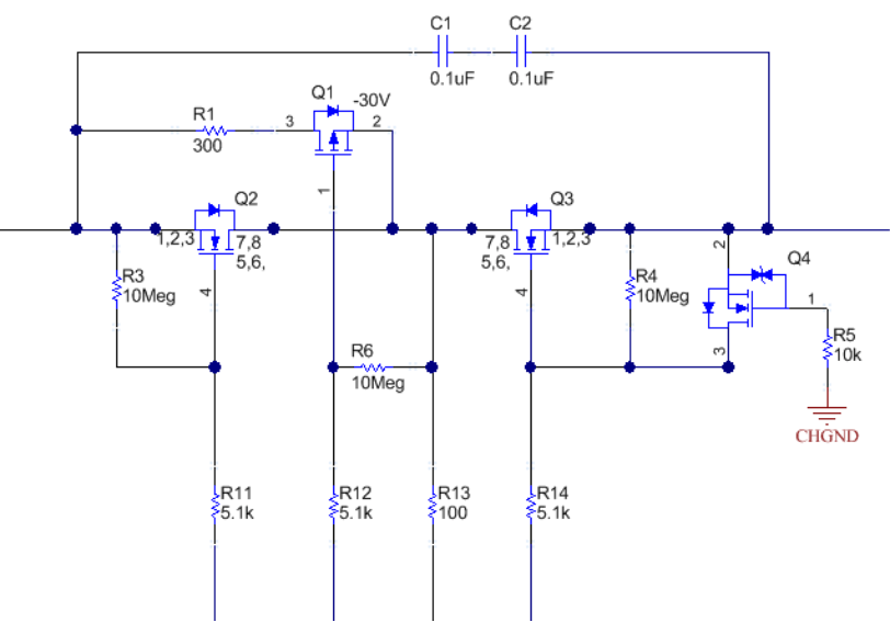
Select the N-channel charge and discharge FETs for a given application. Most portable battery applications are a good match for the CSD17308Q3. The TI CSD17308Q3 is a 47A, 30-V device with Rds(on) of 8.2 mΩ when the gate drive voltage is 8 V.
If a precharge FET is used, R1 is calculated to limit the precharge current to the desired rate. Be sure to account for the power dissipation of the series resistor. The precharge current is limited to (VCHARGER – VBAT)/R1 and maximum power dissipation is (Vcharger – Vbat)2/R1.
The gates of all protection FETs are pulled to the source with a high-value resistor between the gate and source to ensure they are turned off if the gate drive is open.
Capacitors C1 and C2 help protect the FETs during an ESD event. Using two devices ensures normal operation if one becomes shorted. To have good ESD protection, the copper trace inductance of the capacitor leads must be designed to be as short and wide as possible. Ensure that the voltage ratings of both C1 and C2 are adequate to hold off the applied voltage if one of the capacitors becomes shorted.
 Figure 9-2 BQ40Z50-R2 Protection FETs