ZHCSG63C December 2013 – July 2018
PRODUCTION DATA.
- 1 特性
- 2 应用
- 3 说明
- 4 修订历史记录
- 5 Device Comparison Table
- 6 Pin Configuration and Functions
- 7 Specifications
-
8 Detailed Description
- 8.1 Overview
- 8.2 Functional Block Diagram
- 8.3
Feature Description
- 8.3.1 Details of a Qi Wireless Power System and bq51003 Power Transfer Flow Diagrams
- 8.3.2 Dynamic Rectifier Control
- 8.3.3 Dynamic Efficiency Scaling
- 8.3.4 RILIM Calculations
- 8.3.5 Input Overvoltage
- 8.3.6 Adapter Enable Functionality and EN1/EN2 Control
- 8.3.7 End Power Transfer Packet (WPC Header 0x02)
- 8.3.8 Status Outputs
- 8.3.9 WPC Communication Scheme
- 8.3.10 Communication Modulator
- 8.3.11 Adaptive Communication Limit
- 8.3.12 Synchronous Rectification
- 8.3.13 Temperature Sense Resistor Network (TS)
- 8.3.14 3-State Driver Recommendations for the TS-CTRL Pin
- 8.3.15 Thermal Protection
- 8.3.16 WPC v1.2 Compliance – Foreign Object Detection
- 8.4 Device Functional Modes
- 9 Application and Implementation
- 10Power Supply Recommendations
- 11Layout
- 12器件和文档支持
- 13机械、封装和可订购信息
7.6 Typical Characteristics
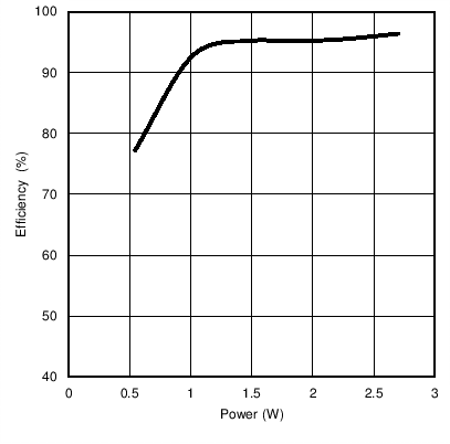 Figure 1. Rectifier Efficiency
 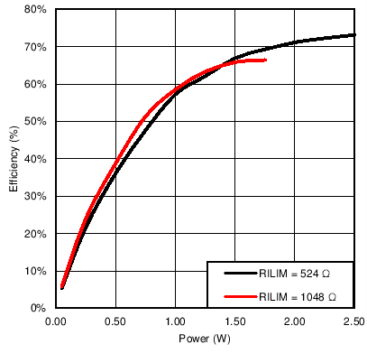 Figure 3. Light Load System Efficiency Improvement Due to Dynamic Efficiency Scaling Feature
 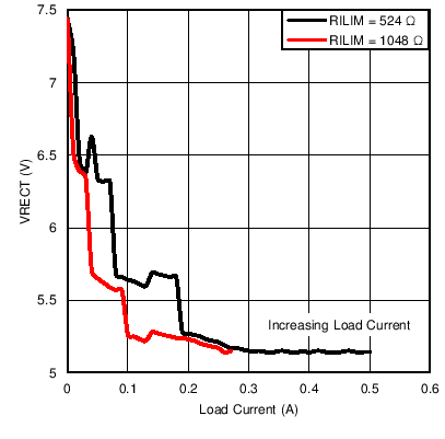 Figure 5. VRECT vs ILOAD at RILIM = 524 Ω and 1048 Ω
 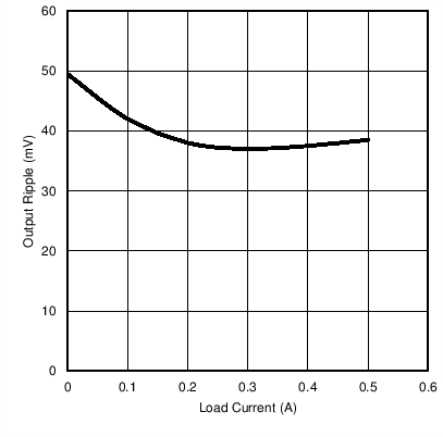 Figure 7. Output Ripple vs ILOAD (COUT = 1 µF) Without Communication
 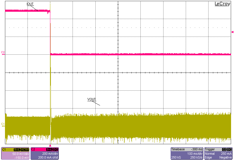 Figure 9. 0.5-A Instantaneous Load Dump
 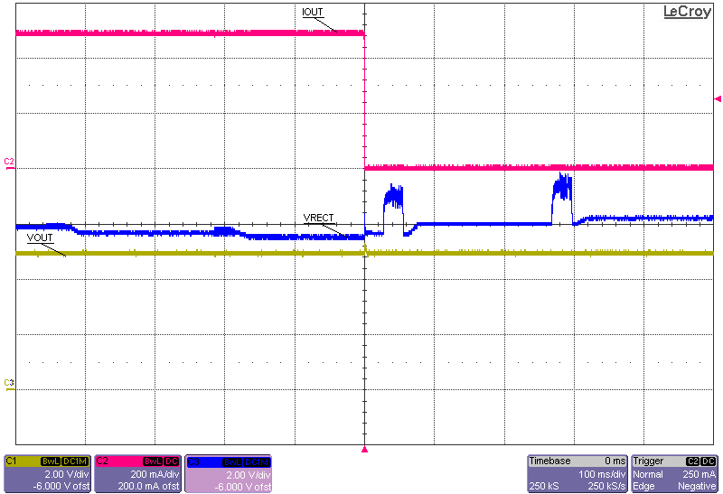 Figure 11. 0.5-A Load Dump Full System Response
 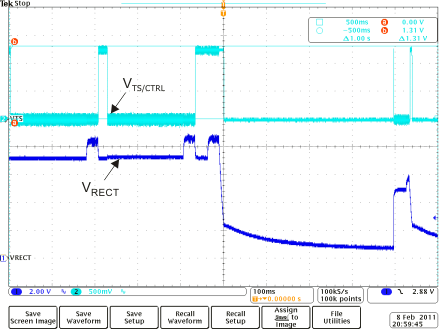 Figure 13. TS Fault
 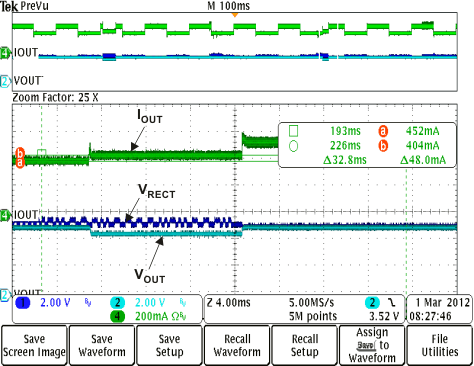 Figure 15. Adaptive Communication Limit Event Where the Current Limit is IOUT + 50 mA (IOUT-DC > 300 mA)
 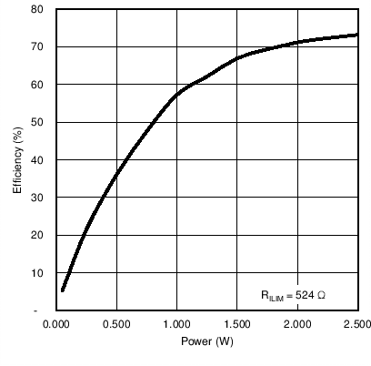 Figure 2. System Efficiency from DC Input to DC Output
 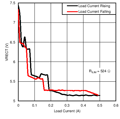 Figure 4. VRECT vs ILOAD at RILIM = 524 Ω
 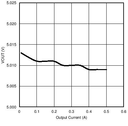 Figure 6. ILOAD Sweep (I-V Curve)
 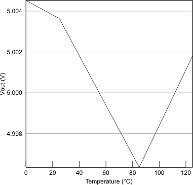 Figure 8. VOUT vs Temperature
 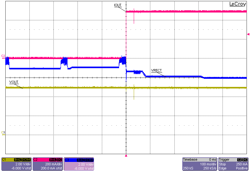 Figure 10. 0.5-A Load Step Full System Response
 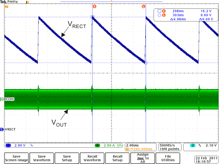 Figure 12. Rectifier Overvoltage Clamp (fop = 110 kHz)
 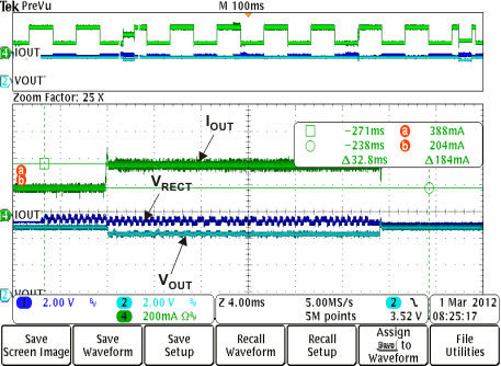 Figure 14. Adaptive Communication Limit Event Where the 400-mA Current Limit is Enabled (IOUT-DC < 300 mA)
 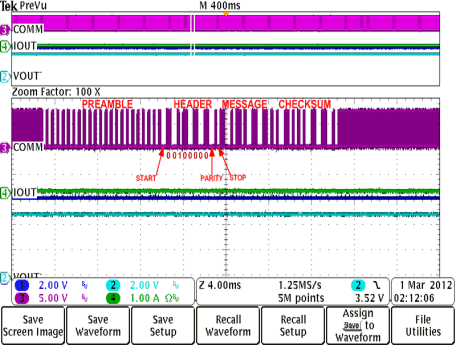 Figure 16. Rx Communication Packet Structure