ZHCSF58A December 2012 – June 2016
PRODUCTION DATA.
- 1 特性
- 2 应用
- 3 说明
- 4 修订历史记录
- 5 Device Comparison Tables
- 6 Pin Configuration and Functions
- 7 Specifications
-
8 Detailed Description
- 8.1 Overview
- 8.2 Functional Block Diagram
- 8.3
Feature Description
- 8.3.1 Qi Wireless Power System and bq51010B Power Transfer Flow Diagrams
- 8.3.2 Dynamic Rectifier Control
- 8.3.3 Dynamic Efficiency Scaling
- 8.3.4 RILIM Calculations
- 8.3.5 Input Overvoltage
- 8.3.6 Adapter Enable Functionality and EN1 or EN2 Control
- 8.3.7 End Power Transfer Packet (WPC Header 0x02)
- 8.3.8 Status Outputs
- 8.3.9 WPC Communication Scheme
- 8.3.10 Communication Modulator
- 8.3.11 Adaptive Communication Limit
- 8.3.12 Synchronous Rectification
- 8.3.13 Temperature Sense Resistor Network (TS)
- 8.3.14 3-State Driver Recommendations For the TS-CTRL Pin
- 8.3.15 Thermal Protection
- 8.3.16 WPC 1.1 Compliance - Foreign Object Detection
- 8.4 Device Functional Modes
-
9 Application and Implementation
- 9.1 Application Information
- 9.2 Typical Applications
- 10Power Supply Recommendations
- 11Layout
- 12器件和文档支持
- 13机械、封装和可订购信息
11 Layout
11.1 Layout Guidelines
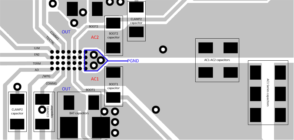
- Keep the trace resistance as low as possible on AC1, AC2, and BAT.
- Detection and resonant capacitors must be as close to the device as possible.
- COMM, CLAMP, and BOOT capacitors must be placed as close to the device as possible.
- Via interconnect on PGND net is critical for appropriate signal integrity and proper thermal performance.
- High-frequency bypass capacitors must be placed close to RECT and OUT pins.
- ILIM and FOD resistors are important signal paths and the loops in those paths to PGND must be minimized.
- AC1 = AC2 = 1.2 A
- OUT = 1 A
- RECT = 100 mA (RMS)
- COMMx = 300 mA
- CLAMPx = 500 mA
- All others can be rated for 10 mA or less
Signal and sensing traces are the most sensitive to noise; the sensing signal amplitudes are usually measured in mV, which is comparable to the noise amplitude. Make sure that these traces are not being interfered by the noisy and power traces. AC1, AC2, BOOT1, BOOT2, COMM1, and COMM2 are the main source of noise in the board. These traces must be shielded from other components in the board. It is usually preferred to have a ground copper area placed underneath these traces to provide additional shielding. Also, make sure they do not interfere with the signal and sensing traces. The PCB must have a ground plane (return) connected directly to the return of all components through vias (two vias per capacitor for power-stage capacitors, one via per capacitor for small-signal components).
For a 1-A fast charge current application, the current rating for each net is as follows:
11.2 Layout Example
 Figure 38. Layout Schematic