ZHCSF58A December 2012 – June 2016
PRODUCTION DATA.
- 1 特性
- 2 应用
- 3 说明
- 4 修订历史记录
- 5 Device Comparison Tables
- 6 Pin Configuration and Functions
- 7 Specifications
-
8 Detailed Description
- 8.1 Overview
- 8.2 Functional Block Diagram
- 8.3
Feature Description
- 8.3.1 Qi Wireless Power System and bq51010B Power Transfer Flow Diagrams
- 8.3.2 Dynamic Rectifier Control
- 8.3.3 Dynamic Efficiency Scaling
- 8.3.4 RILIM Calculations
- 8.3.5 Input Overvoltage
- 8.3.6 Adapter Enable Functionality and EN1 or EN2 Control
- 8.3.7 End Power Transfer Packet (WPC Header 0x02)
- 8.3.8 Status Outputs
- 8.3.9 WPC Communication Scheme
- 8.3.10 Communication Modulator
- 8.3.11 Adaptive Communication Limit
- 8.3.12 Synchronous Rectification
- 8.3.13 Temperature Sense Resistor Network (TS)
- 8.3.14 3-State Driver Recommendations For the TS-CTRL Pin
- 8.3.15 Thermal Protection
- 8.3.16 WPC 1.1 Compliance - Foreign Object Detection
- 8.4 Device Functional Modes
-
9 Application and Implementation
- 9.1 Application Information
- 9.2 Typical Applications
- 10Power Supply Recommendations
- 11Layout
- 12器件和文档支持
- 13机械、封装和可订购信息
9 Application and Implementation
NOTE
Information in the following applications sections is not part of the TI component specification, and TI does not warrant its accuracy or completeness. TI’s customers are responsible for determining suitability of components for their purposes. Customers should validate and test their design implementation to confirm system functionality.
9.1 Application Information
The bq51010B is a fully integrated, wireless power receiver in a single device. The device complies with the WPC v1.1 specifications for a wireless power receiver. When paired with a WPC v1.1 compliant transmitter, the device can provide up to 5-W of power. There are several tools available for the design of the system. These tools may be obtained by checking the product page at www.ti.com/product/bq51010B.
9.2 Typical Applications
9.2.1 bq51010B Wireless Power Receiver Used as a Power Supply
9.2.1.1 Design Requirements
This application is for a system that has varying loads from less than 100 mA up to 1 A. The application must work with any Qi-certified transmitter. There is no requirement for any external thermal measurements. An LED indication is required to indicate an active power supply. Each of the components from the application drawing is examined.
9.2.1.2 Detailed Design Procedure
9.2.1.2.1 Using the bq51010B as a Wireless Power Supply
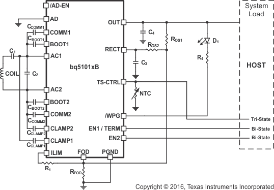
Figure 27 is the schematic of a system which uses the bq51010B as a power supply.
When the system shown in Figure 27 is placed on the charging pad, the receiver coil is inductively coupled to the magnetic flux generated by the coil in the charging pad, which consequently induces a voltage in the receiver coil. The internal synchronous rectifier feeds this voltage to the RECT pin, which has the filter capacitor C3.
The bq51010B identifies and authenticates itself to the primary using the COMM pins by switching on and off the COMM FETs and hence switching in and out CCOMM. If the authentication is successful, the transmitter remains powered on. The bq51010B measures the voltage at the RECT pin, calculates the difference between the actual voltage and the desired voltage VRECT-REG, (threshold 1 at no load) and sends back error packets to the primary. Dynamic VRECT thresholds are shown in Electrical Characteristics. This process goes on until the input voltage settles at VRECT-REG. During a load transient, the dynamic rectifier algorithm sets the targets specified by VRECT-REG thresholds 1, 2, 3, and 4. This algorithm is termed dynamic rectifier control and is used to enhance the transient response of the power supply.
During power up, the LDO is held off until the VRECT-REG threshold 1 converges. The voltage control loop ensures that the output voltage is maintained at VOUT-REG to power the system. The bq51010B meanwhile continues to monitor the input voltage and maintains sending error packets to the primary every 250 ms. If a large overshoot occurs, the feedback to the primary speeds up to every 32 ms to converge on an operating point in less time.
9.2.1.2.2 Series and Parallel Resonant Capacitor Selection
Shown in Figure 27, the capacitors C1 (series) and C2 (parallel) make up the dual resonant circuit with the receiver coil. These two capacitors must be sized correctly per the WPC v1.1 specification. Figure 28 illustrates the equivalent circuit of the dual resonant circuit.
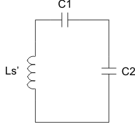 Figure 28. Dual Resonant Circuit With the Receiver Coil
Section 4.2 (Power Receiver Design Requirements) in Part 1 of the WPC v1.1 specification highlights in detail the sizing requirements. To summarize, the receiver designer is required take inductance measurements with a fixed test fixture. Figure 29 shows the test fixture.
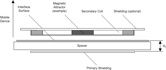 Figure 29. WPC v1.1 Receiver Coil Test Fixture for the Inductance Measurement Ls’ (Copied from System Description Wireless Power Transfer, Volume 1: Low Power, Part 1 Interface Definition,
 Version 1.1)
The primary shield is to be 50 mm × 50 mm × 1 mm of Ferrite material PC44 from TDK Corp. The gap dZ is to be 3.4 mm. The receiver coil, as it is placed in the final system (for example, the back cover and battery must be included if the system calls for this), is to be placed on top of this surface and the inductance is to be measured at 1-V RMS and a frequency of 100 kHz. This measurement is termed Ls’. The same measurement is to be repeated without the test fixture shown in Figure 8. This measurement is termed Ls or the free-space inductance. Each capacitor can then be calculated using Equation 5.
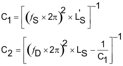
where
- fS is 100 kHz +5/-10%
- fD is 1 MHz ±10%
C1 must be chosen first prior to calculating C2.
The quality factor must be greater than 77 and can be determined by Equation 6.

where
- R is the DC resistance of the receiver coil
All other constants are defined above.
9.2.1.2.3 COMM, CLAMP, and BOOT Capacitors
For most applications, the COMM, CLAMP, and BOOT capacitance values is chosen to match the bq51010B.
The BOOT capacitors are used to allow the internal rectifier FETs to turn on and off properly. These capacitors are from AC1 to BOOT1 and from AC2 to BOOT2 and must have a minimum 25-V rating. A 10-nF capacitor with a 25-V rating is chosen.
The CLAMP capacitors are used to aid in the clamping process to protect against overvoltage. These capacitors are from AC1 to CLAMP1 and from AC2 to CLAMP2 and must have a minimum 25-V rating. A 0.47-µF capacitor with a 25-V rating is chosen.
The COMM capacitors are used to facilitate the communication from the RX to the TX. This selection can vary a bit more than the BOOT and CLAMP capacitors. In general, TI recommends a 22-nF capacitor. Based on the results of testing of the communication robustness in the final solution, a change to a 47-nF capacitor may be in order. The larger the capacitor the larger the deviation is on the coil which sends a stronger signal to the TX. This also decreases the efficiency somewhat. In this case, a 22-nF capacitor with a 25-V rating is chosen.
9.2.1.2.4 Control Pins and WPG
This section discusses the pins that control the functions of the bq51010B (AD, AD_EN, EN1, EN2, and TS or CTRL).
This solution uses wireless power exclusively. The AD pin is tied low to disable wired power interaction. The output pin AD_EN is left floating.
EN1 and EN2 are tied to the system controller GPIO pins. This allows the system to control the wireless power transfer. Normal operation leaves EN1 and EN2 low or floating (GPIO low or high impedance). EN1 and EN2 have internal pulldown resistors. With both EN1 and EN2 low, wireless power is enabled and power can be transferred whenever the RX is on a suitable TX. The RX system controller can terminate power transfer and send an EPT 0x01 (Charge Complete) by setting EN1=EN2=1. The TX terminates power when the EPT 0x01 is received. The TX continues to test for power transfer, but not engage until the RX requests power. For example, if the TX is the bq500212A, the TX sends digital pings approximately once per 5 seconds. During each ping, the bq51010B resends the EPT 0x01. Between the pings, the bq500212A goes into low power sleep mode reducing power consumption. When the RX system controller determines it is time to resume power transfer (for example, the battery voltage is below its recharge threshold) the controller simply returns EN1 and EN2 to low (or float) states. The next ping of the bq500212A powers the bq51010B which now communicates that it is time to transfer power. The TX and RX communication resumes and power transfer is reinitiated.
The TS or CTRL pin is used as a temperature sensor (with the NTC) and maintain the ability to terminate power transfer through the system controller. In this case, the GPIO is in high impedance for normal NTC (Temperature Sense) control.
The WPG pin is used to indicate power transfer. A 2.1-V forward bias LED is used for D1 with a current limiting 1.5-kΩ series resistor. The LED and resistor are tied from OUT to PGND and D1 lights during power transfer.
9.2.1.2.5 Current Limit and FOD
The current limit and foreign object detection functions are related. The current limit is set by R1 + RFOD. RFOD and Ros are determined by FOD calibration. Default values of 20 kΩ for Ros (to RECT, Ros2. Ros1 is not populated). 200 Ω for RFOD are used. The final values required to be determined based on the FOD calibration. The tool for FOD calibration can be found on the bq51010B web folder under Tools & Software. Good practice is to set the layout with 2 resistors for Ros and 2 for RFOD to allow for precise values once the calibration is complete.
After setting RFOD, R1 can be calculated based on the desired current limit. The maximum current for this solution under normal operating conditions (IMAX) is 714 mA. Using Equation 1 to calculate the maximum current yields a value of 367 Ω for RILIM. With RFOD set to 200 Ω the remaining resistance for R1 is 167 Ω. Choose the closest standard resistor of 165 Ω. This also sets the hardware current limit to 856 mA to allow for temporary current surges without system performance concerns.
9.2.1.2.6 RECT and OUT Capacitance
RECT capacitance is used to smooth the AC to DC conversion and to prevent minor current transients from passing to OUT. For this 714-mA IMAX, select two 10-µF capacitors and one 0.1-µF capacitor. These must be rated to 16 V.
OUT capacitance is used to reduce any ripple from minor load transients. For this solution, a single 10-µF capacitor and a single 0.1-µF capacitor are used.
9.2.1.3 Application Curves
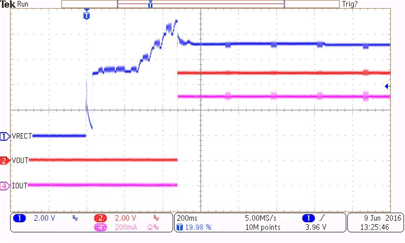 Figure 30. Start-Up With 700-mA Load
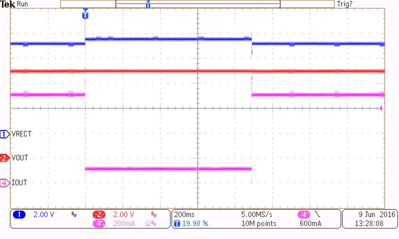 Figure 31. Load Transitions (0.7 A to 0.1 A to 0.7 A)
9.2.2 Dual Power Path: Wireless Power and DC Input
9.2.2.1 Design Requirements
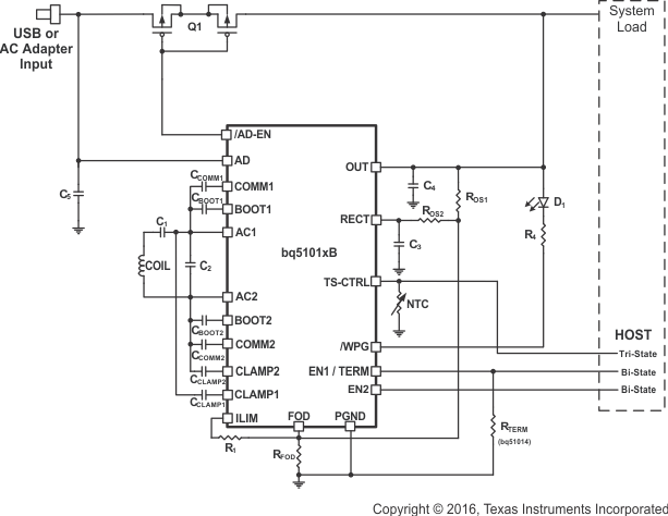
This solution adds the ability to disable wireless charging with the AD and AD_EN pins. A DC supply (USB or AC adapter with DC output) can also be used to power the subsystem. This can occur during wireless power transfer or without wireless power transfer. The system must allow power transfer without any backflow or damage to the circuitry.
9.2.2.2 Detailed Design Procedure
The basic components used in Figure 27 are reused here in Figure 32. The additional circuitry needed for source control will be discussed. Adding a blocking FET while using the bq51010B for control is the only addition to the circuitry. The AD pin is tied to the DC input as a threshold detector. The AD_EN pin is used to enable or disable the blocking FET. The blocking FET must be chosen to handle the appropriate current level and the DC voltage level supplied from the input. In this example, the expectation is that the DC input is 7 V with a maximum current of 700 mA (same configuration as the wireless power supply). The CSD75207W15 is a good fit because it is a P-Channel, –20-V, 3.9-A FET pair in a 1.5-mm2 WCSP.
9.2.2.3 Application Curves
The following scope plots show behavior under different conditions.
Figure 33 shows the transition from wireless power to wired power when power is added to the AD pin. VRECT drops and there is a short time (IOUT drops to zero) when neither source is providing power. When Q1 is enabled (through AD_EN) the output current turns back on. Note the RECT voltage after about 500 ms. This is the TX sending a ping to check to see if power is required. RECT returns to low after the bq51010B informs the TX it does not required power (without enabling the OUT pin). This timing is based on the TX (bq500212A used here).
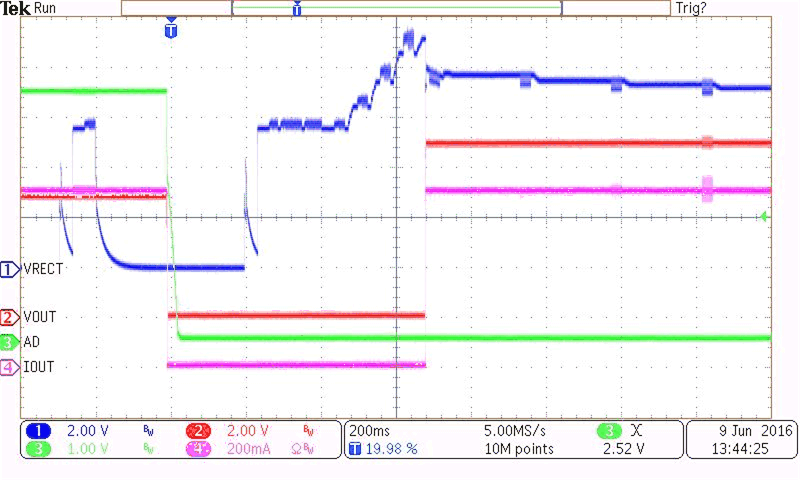
Figure 34 shows the transition to wireless power when the AD voltage is removed. Note that after wired power is removed, the next ping from bq500212A energizes the bq51010B. Once the rectifier voltage is stable the output turns on.
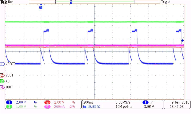
Figure 35 shows a system placed onto the transmitter with AD already powered. The TX sends a ping which the RX responds to and informs the TX that no power is required. The ping continues with the timing based on the TX used.
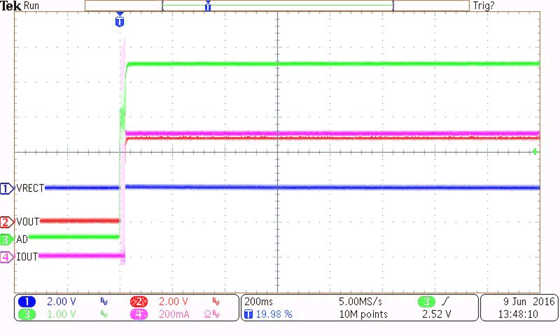
Figure 36 shows the AD added when the RX is not on a TX. This indicates normal start-up without requirement of the TX.
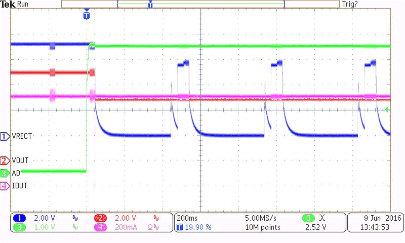
| CH1: VRECT | CH2: VOUT | |
| CH3: VAD | CH4: IOUT |
| CH1: VRECT | CH2: VOUT | |
| CH3: VAD | CH4: IOUT |
(EN1 = EN2 = LOW)
| CH1: VRECT | CH2: VOUT | |
| CH3: VAD | CH4: IOUT |
| CH1: VRECT | CH2: VOUT | |
| CH3: VAD | CH4: IOUT |
(EN1 = EN2 = LOW)
9.2.3 Wireless and Direct Charging of a Li-Ion Battery at 800 mA
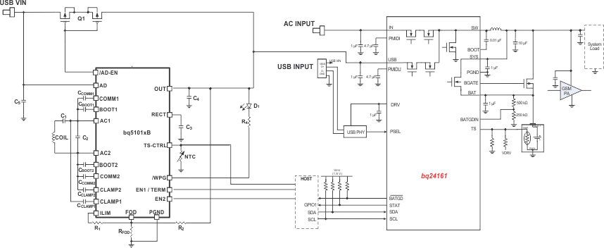 Figure 37. bq51010B Used as a Wireless Power Supply With Adapter Multiplexing on a Two Input Charger
9.2.3.1 Design Requirements
The goal of this design is to charge a 3.7-V Li-Ion battery at 800 mA either wirelessly or with a direct USB wired input. This design will use the bq51010B wireless power supply and the bq24161 single-cell Li-Ion battery charger. A low resistance path has to be created between the output of bq51010B and the input of bq24161.
9.2.3.2 Detailed Design Procedure
The basic components used in Figure 27 and Figure 32 are reused in Figure 37, as well. The bq51010B OUT pin is tied to the output of Q1 and directly to the IN pin of the bq24040. No other changes to the bq51010B circuitry are required. Consult the bq24161 data sheet bq2416xx 2.5A, Dual-Input, Single-Cell Switched-Mode Li-Ion Battery Charger with Power Path Management and I2C Interface for selecting its correct components.