ZHCSM89 july 2021 BQ51013B-Q1
PRODUCTION DATA
- 1
- 1 特性
- 2 应用
- 3 说明
- 4 Revision History
- 5 Description (continued)
- 6 Device Comparison Table
- 7 Pin Configuration and Functions
- 8 Specifications
-
9 Detailed Description
- 9.1 Overview
- 9.2 Functional Block Diagram
- 9.3
Feature Description
- 9.3.1 Details of a Qi Wireless Power System and BQ51013B-Q1 Power Transfer Flow Diagrams
- 9.3.2 Dynamic Rectifier Control
- 9.3.3 Dynamic Efficiency Scaling
- 9.3.4 RILIM Calculations
- 9.3.5 Input Overvoltage
- 9.3.6 Adapter Enable Functionality and EN1/EN2 Control
- 9.3.7 End Power Transfer Packet (WPC Header 0x02)
- 9.3.8 Status Outputs
- 9.3.9 WPC Communication Scheme
- 9.3.10 Communication Modulator
- 9.3.11 Adaptive Communication Limit
- 9.3.12 Synchronous Rectification
- 9.3.13 Temperature Sense Resistor Network (TS)
- 9.3.14 3-State Driver Recommendations for the TS/CTRL Pin
- 9.3.15 Thermal Protection
- 9.3.16 WPC v1.2 Compliance – Foreign Object Detection
- 9.3.17 Receiver Coil Load-Line Analysis
- 9.4 Device Functional Modes
-
10Application and Implementation
- 10.1 Application Information
- 10.2
Typical Applications
- 10.2.1
BQ51013B-Q1 Wireless Power Receiver Used as a Power
Supply
- 10.2.1.1 Design Requirements
- 10.2.1.2
Detailed Design Procedure
- 10.2.1.2.1 Using The BQ51013B-Q1 as a Wireless Power Supply: (See )
- 10.2.1.2.2 Series and Parallel Resonant Capacitor Selection
- 10.2.1.2.3 Recommended RX Coils
- 10.2.1.2.4 COMM, CLAMP, and BOOT Capacitors
- 10.2.1.2.5 Control Pins and CHG
- 10.2.1.2.6 Current Limit and FOD
- 10.2.1.2.7 RECT and OUT Capacitance
- 10.2.1.3 Application Curves
- 10.2.2 Dual Power Path: Wireless Power and DC Input
- 10.2.3 Wireless and Direct Charging of a Li-Ion Battery at 800 mA
- 10.2.1
BQ51013B-Q1 Wireless Power Receiver Used as a Power
Supply
- 11Power Supply Recommendations
- 12Layout
- 13Device and Documentation Support
- 14Mechanical, Packaging, and Orderable Information
9.3.4 RILIM Calculations
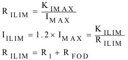
The BQ51013B-Q1 includes a means of providing hardware overcurrent protection by means of an analog current regulation loop. The hardware current limit provides an extra level of safety by clamping the maximum allowable output current (current compliance). The RILIM resistor size also sets the thresholds for the dynamic rectifier levels and thus providing efficiency tuning per each application’s maximum system current. The calculation for the total RILIM resistance is as follows:

where
- IMAX is the expected maximum output current during normal operation.
- IILIM is the hardware over current limit.
When referring to the application diagram shown in Figure 10-1, RILIM is the sum of RFOD and R1 (the total resistance from the ILIM pin to GND).