ZHCSM89 july 2021 BQ51013B-Q1
PRODUCTION DATA
- 1
- 1 特性
- 2 应用
- 3 说明
- 4 Revision History
- 5 Description (continued)
- 6 Device Comparison Table
- 7 Pin Configuration and Functions
- 8 Specifications
-
9 Detailed Description
- 9.1 Overview
- 9.2 Functional Block Diagram
- 9.3
Feature Description
- 9.3.1 Details of a Qi Wireless Power System and BQ51013B-Q1 Power Transfer Flow Diagrams
- 9.3.2 Dynamic Rectifier Control
- 9.3.3 Dynamic Efficiency Scaling
- 9.3.4 RILIM Calculations
- 9.3.5 Input Overvoltage
- 9.3.6 Adapter Enable Functionality and EN1/EN2 Control
- 9.3.7 End Power Transfer Packet (WPC Header 0x02)
- 9.3.8 Status Outputs
- 9.3.9 WPC Communication Scheme
- 9.3.10 Communication Modulator
- 9.3.11 Adaptive Communication Limit
- 9.3.12 Synchronous Rectification
- 9.3.13 Temperature Sense Resistor Network (TS)
- 9.3.14 3-State Driver Recommendations for the TS/CTRL Pin
- 9.3.15 Thermal Protection
- 9.3.16 WPC v1.2 Compliance – Foreign Object Detection
- 9.3.17 Receiver Coil Load-Line Analysis
- 9.4 Device Functional Modes
-
10Application and Implementation
- 10.1 Application Information
- 10.2
Typical Applications
- 10.2.1
BQ51013B-Q1 Wireless Power Receiver Used as a Power
Supply
- 10.2.1.1 Design Requirements
- 10.2.1.2
Detailed Design Procedure
- 10.2.1.2.1 Using The BQ51013B-Q1 as a Wireless Power Supply: (See )
- 10.2.1.2.2 Series and Parallel Resonant Capacitor Selection
- 10.2.1.2.3 Recommended RX Coils
- 10.2.1.2.4 COMM, CLAMP, and BOOT Capacitors
- 10.2.1.2.5 Control Pins and CHG
- 10.2.1.2.6 Current Limit and FOD
- 10.2.1.2.7 RECT and OUT Capacitance
- 10.2.1.3 Application Curves
- 10.2.2 Dual Power Path: Wireless Power and DC Input
- 10.2.3 Wireless and Direct Charging of a Li-Ion Battery at 800 mA
- 10.2.1
BQ51013B-Q1 Wireless Power Receiver Used as a Power
Supply
- 11Power Supply Recommendations
- 12Layout
- 13Device and Documentation Support
- 14Mechanical, Packaging, and Orderable Information
9.3.17 Receiver Coil Load-Line Analysis
When choosing a receiver coil, TI recommends analyzing the transformer characteristics between the primary coil and receiver coil through load-line analysis. This will capture two important conditions in the WPC system:
- Operating point characteristics in the closed loop of the WPC system.
- Instantaneous transient response prior to the convergence of the new operating point.
An example test configuration for conducting this analysis is shown in Figure 9-16:
 Figure 9-16 Load-Line Analysis Test Bench
Where:
- VIN is a square-wave power source that should have a peak-to-peak operation of 19 V.
- CP is the primary series resonant capacitor (for example, 100 nF for Type A1 coil).
- LP is the primary coil of interest (such as, Type A1).
- LS is the secondary coil of interest.
- CS is the series resonant capacitor chosen for the receiver coil under test.
- CD is the parallel resonant capacitor chosen for the receiver coil under test.
- CB is the bulk capacitor of the diode bridge (voltage rating should be at least 25 V and capacitance value of at least 10 µF)
- V is a Kelvin connected voltage meter
- A is a series ammeter
- RL is the load of interest
TI recommends that the diode bridge be constructed of Schottky diodes.
The test procedure is as follows
- Supply a 19-V AC signal to LP starting at a frequency of 210 kHz
- Measure the resulting rectified voltage from no load to the expected full load
- Repeat the above steps for lower frequencies (stopping at 110 kHz)
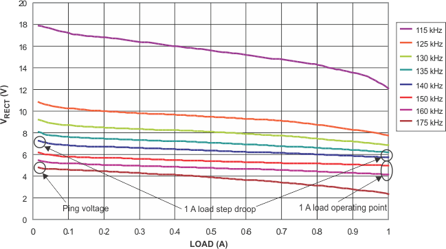
An example load-line analysis is shown in Figure 9-17:
 Figure 9-17 Example Load-Line Results
What Figure 9-17 conveys about the operating point is that a specific load and rectifier target condition consequently results in a specific operating frequency (for the type A1 TX). For example, at 1 A the dynamic rectifier target is 5.15 V. Therefore, the operating frequency will be from 150 kHz to 160 kHz in the above example. This is an acceptable operating point. If the operating point ever falls outside the WPC frequency range (110 kHz – 205 kHz), the system will never converge and will become unstable.
In regards to transient analysis, there are two major points of interest:
- Rectifier voltage at the ping frequency (175 kHz).
- Rectifier voltage droop from no load to full load at the constant operating point.
In this example, the ping voltage will be approximately 5 V. This is above the UVLO of the BQ51013B-Q1 and, therefore, start-up in the WPC system can be ensured. If the voltage is near or below the UVLO at this frequency, then start-up in the WPC system may not occur.
If the maximum load step is 1 A, the droop in this example will be approximately 1 V (using the 140 kHz load-line). To analyze the droop, locate the load-line that starts at 7 V at no-load. Follow this load-line to the maximum load expected and take the difference between the 7-V no-load voltage and the full-load voltage at that constant frequency. Ensure that the full-load voltage at this constant frequency is above 5 V. If it descends below 5 V, the output of the power supply will also droop to this level. This type of transient response analysis is necessary due to the slow feedback response of the WPC system. This simulates the step response prior to the WPC system adjusting the operating point.
Coupling between the primary and secondary coils will worsen with misalignment of the secondary coil. Therefore, it is recommended to re-analyze the load-lines at multiple misalignments to determine where, in planar space, the receiver will discontinue operation.
See Table 10-1 for recommended RX coils.