ZHCSVT2A April 2022 – April 2024 BQ76922
PRODUCTION DATA
- 1
- 1 特性
- 2 应用
- 3 说明
- 4 Device Comparison Table
- 5 Pin Configuration and Functions
-
6 Specifications
- 6.1 Absolute Maximum Ratings
- 6.2 ESD Ratings
- 6.3 Recommended Operating Conditions
- 6.4 Thermal Information BQ76922
- 6.5 Supply Current
- 6.6 Digital I/O
- 6.7 LD Pin
- 6.8 Precharge (PCHG) and Predischarge (PDSG) FET Drive
- 6.9 FUSE Pin Functionality
- 6.10 REG18 LDO
- 6.11 REG0 Pre-regulator
- 6.12 REG1 LDO
- 6.13 Voltage References
- 6.14 Coulomb Counter
- 6.15 Coulomb Counter Digital Filter (CC1)
- 6.16 Current Measurement Digital Filter (CC2)
- 6.17 Current Wake Detector
- 6.18 Analog-to-Digital Converter
- 6.19 Cell Balancing
- 6.20 Cell Open Wire Detector
- 6.21 Internal Temperature Sensor
- 6.22 Thermistor Measurement
- 6.23 Internal Oscillators
- 6.24 High-side NFET Drivers
- 6.25 Comparator-Based Protection Subsystem
- 6.26 Timing Requirements – I2C Interface, 100kHz Mode
- 6.27 Timing Requirements – I2C Interface, 400kHz Mode
- 6.28 Timing Requirements – HDQ Interface
- 6.29 Interface Timing Diagrams
- 6.30 Typical Characteristics
-
7 Detailed Description
- 7.1 Overview
- 7.2 Functional Block Diagram
- 7.3 Diagnostics
- 7.4 Device Configuration
- 7.5
Measurement Subsystem
- 7.5.1 Voltage Measurement
- 7.5.2 General Purpose ADCIN Functionality
- 7.5.3 Coulomb Counter and Digital Filters
- 7.5.4 Synchronized Voltage and Current Measurement
- 7.5.5 Internal Temperature Measurement
- 7.5.6 Thermistor Temperature Measurement
- 7.5.7 Factory Trim of Voltage ADC
- 7.5.8 Voltage Calibration (ADC Measurements)
- 7.5.9 Voltage Calibration (COV and CUV Protections)
- 7.5.10 Current Calibration
- 7.5.11 Temperature Calibration
- 7.6 Primary and Secondary Protection Subsystems
- 7.7
Device
Hardware Features
- 7.7.1 Voltage References
- 7.7.2 ADC Multiplexer
- 7.7.3 LDOs
- 7.7.4 Standalone Versus Host Interface
- 7.7.5 Multifunction Pin Controls
- 7.7.6 RST_SHUT Pin Operation
- 7.7.7 CFETOFF, DFETOFF, and BOTHOFF Pin Functionality
- 7.7.8 ALERT Pin Operation
- 7.7.9 Fuse Drive
- 7.7.10 Cell Open Wire
- 7.7.11 Low Frequency Oscillator
- 7.7.12 High Frequency Oscillator
- 7.8 Device Functional Modes
- 7.9 Serial Communications Interface
- 7.10 Cell Balancing
- 8 Application and Implementation
- 9 Power Supply Requirements
- 10Layout
- 11Device and Documentation Support
- 12Revision History
- 13Mechanical, Packaging, Orderable Information
8.2 Typical Applications
A simplified application schematic for a 5-series battery pack is shown in Figure 8-1, using the BQ76922 together with an external secondary protector and a host microcontroller. This configuration uses CHG and DSG FETs in series, together with high-side PFET devices used to implement precharge and predischarge functionality. Several points to consider in an implementation are included below:
- The external NPN BJT used for the REGIN preregulator can be configured with its collector routed either to the cell battery stack or the middle of the protection FETs.
- A diode is recommended in the drain circuit of the external NPN BJT, which avoids reverse current flow from the BREG pin through the BJT base to collector in the event of a pack short circuit. This diode can be a Schottky diode if low voltage pack operation is needed, or a conventional diode can be used otherwise.
- A series diode is recommended at the BAT pin, together with a capacitor from the pin to VSS. These components allow the device to continue operating for a short time when a pack short circuit occurs, which may cause the PACK+ and top-of-stack voltages to drop to approximately 0V. In this case, the diode prevents the BAT pin from being pulled low with the stack, and the device will continue to operate, drawing current from the capacitor. Generally operation is only required for a short time, until the device detects the short circuit event and disables the DSG FET. A Schottky diode can be used if low voltage pack operation is needed, or a conventional diode can be used otherwise.
- The diode in the BAT connection and the diode in the BJT collector should not be shared, since then the REG0 circuit might discharge the capacitor on BAT too quickly during a short circuit event.
- The recommended voltage range on the VC0 to VC3A pins extends to –0.2V. This can be used, for example, to measure a differential voltage that extends slightly below ground, such as the voltage across a second sense resistor in parallel with that connected to the SRP and SRN pins.
- If a system does not use high-side protection FETs, then the PACK pin can be connected through a series 10kΩ resistor to the top of stack. The LD pin can be connected to VSS. In this case, the LD pin can also be controlled separately, in order to wake the device from SHUTDOWN mode, such as through external circuitry which holds the LD pin at the voltage of VSS while the device stays in SHUTDOWN, and to be driven above a voltage of VWAKEONLD in order to wake from SHUTDOWN.
- TI recommends using 100Ω resistors in series with the SRP and SRN pins, and a 100nF with optional 100pF differential filter capacitance between the pins for filtering. The routing of these components, together with the sense resistor, to the pins should be minimized and fully symmetric, with all components recommended to stay on the same side of the PCB with the device. Capacitors should not be connected from the pins to VSS.
- Due to thermistors often being attached to cells and possibly needing long wires to connect back to the device, it may be helpful to add a capacitor from the thermistor pin to the device VSS. However, it is important to not use too large of a value of capacitor, since this will affect the settling time when the thermistor is biased and measured periodically. A rule of thumb is to keep the time constant of the circuit < 5% of the measurement time. When Settings:Configuration:Power Config[FASTADC] = 0, the measurement time is approximately 3 ms, and with [FASTADC] = 1 the measurement time is halved to approximately 1.5ms. When using the 18kΩ pullup resistor with the thermistor, the time constant will generally be less than (18kΩ) × C, so a capacitor less than 4nF is recommended. When using the 180kΩ pullup resistor, the capacitor should be less than 400pF.
- The integrated charge pump generates a voltage on the CP1 capacitor, requiring approximately 60ms to charge up to approximately 11V when first enabled, when using the recommended 470nF capacitor value. When the CHG or DSG drivers are enabled, charge redistribution occurs from the CP1 capacitor to the CHG and DSG capacitive FET loads. This will generally result in a brief drop in the voltage on CP1, which is then replenished by the charge pump. If the FET capacitive loading is large, such that at FET turn-on the voltage on CP1 drops below an acceptable level for the application, then the value of the CP1 capacitor can be increased. This has the drawback of requiring a longer startup time for the voltage on CP1 when the charge pump is first powered on, and so should be evaluated to ensure it is acceptable in the system. For example, if the CHG and DSG FETs are enabled simultaneously and their combined gate capacitance is approximately 400nF, then changing CP1 to a value of 2200nF will result in the 11V charge pump level dropping to approximately 9V, before being restored to the 11V level by the charge pump.
 Figure 8-1 BQ76922 5-Series
Cell Typical Implementation (Simplified Schematic)
Figure 8-1 BQ76922 5-Series
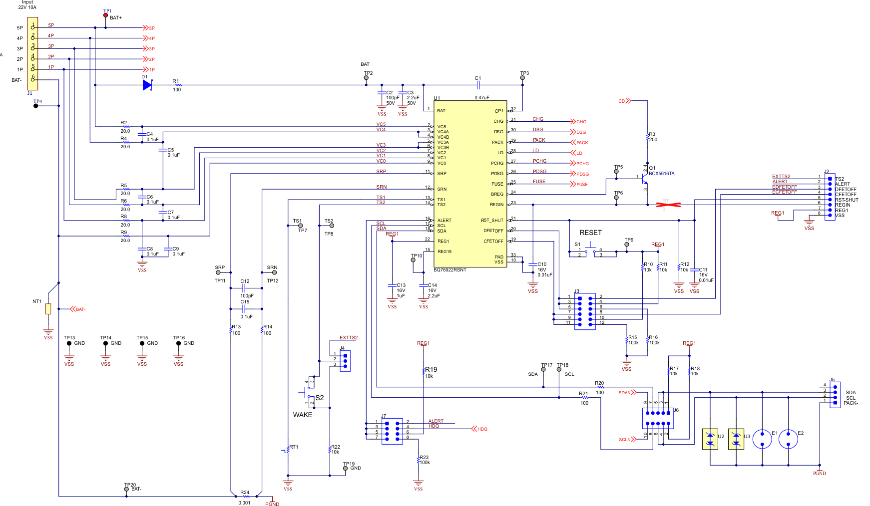
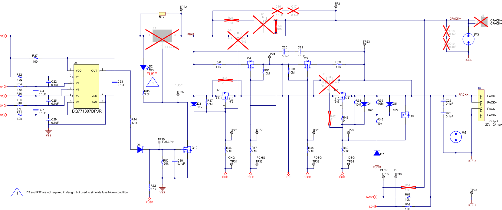
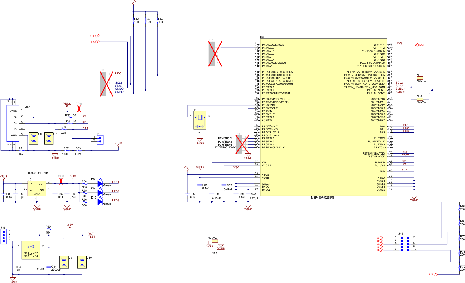
Cell Typical Implementation (Simplified Schematic)A full schematic of a basic monitor circuit based on the BQ76922 for a 5-series battery pack is shown below. The board layout for this design is shown in Section 10.2.

Figure 8-2 BQ76922 5-Series Cell Schematic Diagram—Monitor

Figure 8-3 BQ76922 5-Series Cell Schematic Diagram—Additional Circuitry
 Figure 8-4 BQ76922 5-Series Cell Schematic
Diagram—Interface Adapter