ZHCSVT2A April 2022 – April 2024 BQ76922
PRODUCTION DATA
- 1
- 1 特性
- 2 应用
- 3 说明
- 4 Device Comparison Table
- 5 Pin Configuration and Functions
-
6 Specifications
- 6.1 Absolute Maximum Ratings
- 6.2 ESD Ratings
- 6.3 Recommended Operating Conditions
- 6.4 Thermal Information BQ76922
- 6.5 Supply Current
- 6.6 Digital I/O
- 6.7 LD Pin
- 6.8 Precharge (PCHG) and Predischarge (PDSG) FET Drive
- 6.9 FUSE Pin Functionality
- 6.10 REG18 LDO
- 6.11 REG0 Pre-regulator
- 6.12 REG1 LDO
- 6.13 Voltage References
- 6.14 Coulomb Counter
- 6.15 Coulomb Counter Digital Filter (CC1)
- 6.16 Current Measurement Digital Filter (CC2)
- 6.17 Current Wake Detector
- 6.18 Analog-to-Digital Converter
- 6.19 Cell Balancing
- 6.20 Cell Open Wire Detector
- 6.21 Internal Temperature Sensor
- 6.22 Thermistor Measurement
- 6.23 Internal Oscillators
- 6.24 High-side NFET Drivers
- 6.25 Comparator-Based Protection Subsystem
- 6.26 Timing Requirements – I2C Interface, 100kHz Mode
- 6.27 Timing Requirements – I2C Interface, 400kHz Mode
- 6.28 Timing Requirements – HDQ Interface
- 6.29 Interface Timing Diagrams
- 6.30 Typical Characteristics
-
7 Detailed Description
- 7.1 Overview
- 7.2 Functional Block Diagram
- 7.3 Diagnostics
- 7.4 Device Configuration
- 7.5
Measurement Subsystem
- 7.5.1 Voltage Measurement
- 7.5.2 General Purpose ADCIN Functionality
- 7.5.3 Coulomb Counter and Digital Filters
- 7.5.4 Synchronized Voltage and Current Measurement
- 7.5.5 Internal Temperature Measurement
- 7.5.6 Thermistor Temperature Measurement
- 7.5.7 Factory Trim of Voltage ADC
- 7.5.8 Voltage Calibration (ADC Measurements)
- 7.5.9 Voltage Calibration (COV and CUV Protections)
- 7.5.10 Current Calibration
- 7.5.11 Temperature Calibration
- 7.6 Primary and Secondary Protection Subsystems
- 7.7
Device
Hardware Features
- 7.7.1 Voltage References
- 7.7.2 ADC Multiplexer
- 7.7.3 LDOs
- 7.7.4 Standalone Versus Host Interface
- 7.7.5 Multifunction Pin Controls
- 7.7.6 RST_SHUT Pin Operation
- 7.7.7 CFETOFF, DFETOFF, and BOTHOFF Pin Functionality
- 7.7.8 ALERT Pin Operation
- 7.7.9 Fuse Drive
- 7.7.10 Cell Open Wire
- 7.7.11 Low Frequency Oscillator
- 7.7.12 High Frequency Oscillator
- 7.8 Device Functional Modes
- 7.9 Serial Communications Interface
- 7.10 Cell Balancing
- 8 Application and Implementation
- 9 Power Supply Requirements
- 10Layout
- 11Device and Documentation Support
- 12Revision History
- 13Mechanical, Packaging, Orderable Information
7.9.2 I2C Communications
The I2C serial communications interface in the BQ76922 device acts as a responder device and supports rates up to 400kHz with an optional CRC check. If the OTP has not been programmed, the BQ76922 device will initially power up by default in 400kHz I2C mode. The OTP setting can be programmed on the manufacturing line, then when the device powers up, it will automatically enter the selected mode per OTP setting. The host can also change the I2C speed setting while in CONFIG_UPDATE mode, then the new speed setting will take effect upon exit of CONFIG_UPDATE mode. Alternatively, the host can use the SWAP_TO_I2C() subcommand to change the communications interface to I2C immediately.
The I2C device address (as an 8bit value including responder address and R/W bit) is set by default as 0x10 (write), 0x11 (read), which can be changed by configuration setting.
The communications interface includes programmable timeout capability, this should only be used if the bus will be operating at 100kHz or 400kHz. If this is enabled with the device set to 100kHz mode, then the device will reset the communications interface logic if a clock is detected low longer than a tTIMEOUT of 25ms to 35ms, or if the cumulative clock low responder extend time exceeds approximately 25ms, or if the cumulative clock low controller extend time exceeds 10ms. If the timeouts are enabled with the device set to 400kHz mode, then the device will reset the communications interface logic if a clock is detected low longer than tTIMEOUT of 5ms to 20ms. The bus also includes a long-term timeout if the SCL pin is detected low for more than 2 seconds, which applies whether or not the timeouts above are enabled.
An I2C write transaction is shown in I2C Write. Block writes are allowed by sending additional data bytes before the Stop. The I2C logic will auto-increment the register address after each data byte.
When enabled, the CRC is calculated as follows:
- Note that the CRC is reset after each data byte and after each stop.
- In a single-byte write transaction, the CRC is calculated over the responder address, register address, and data.
- In a block write transaction, the CRC for the first data byte is calculated over the responder address, register address, and data. The CRC for subsequent data bytes is calculated over the data byte only.
The CRC polynomial is x8 + x2 + x + 1, and the initial value is 0.
When the responder detects an invalid CRC, the I2C responder will NACK the CRC, which causes the I2C responder to go to an idle state.

Figure 7-6 I2C Write
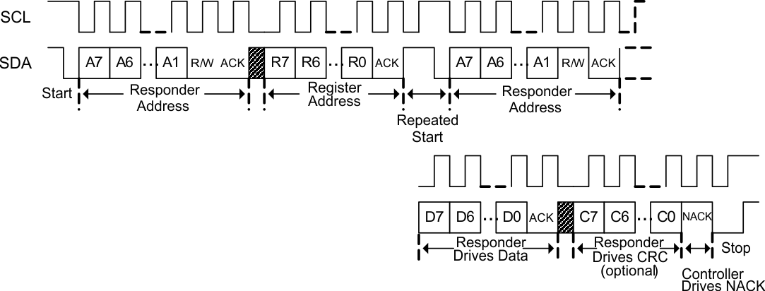
I2C Read with Repeated Start shows a read transaction using a Repeated Start.

Figure 7-7 I2C Read with Repeated Start
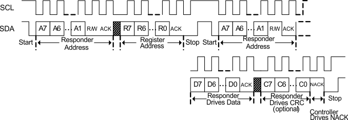
I2C Read without Repeated Start shows a read transaction where a Repeated Start is not used, for example if not available in hardware. For a block read, the controller ACK’s each data byte except the last and continues to clock the interface. The I2C block will auto-increment the register address after each data byte.
When enabled, the CRC for a read transaction is calculated as follows:
- Note that the CRC is reset after each data byte and after each stop.
- In a single-byte read transaction using a repeated start, the CRC is calculated beginning at the first start, so will include the responder address, the register address, then the responder address with read bit set, then the data byte.
- In a single-byte read transaction using a stop after the initial register address, the CRC is reset after the stop, so will only include the responder address with read bit set and the data byte.
- In a block read transaction using repeated starts, the CRC for the first data byte is calculated beginning at the first start and will include the responder address, the register address, then the responder address with read bit set, then the data byte. The CRC for subsequent data bytes is calculated over the data byte only.
- In a block read transaction using a stop after the initial register address, the CRC is reset after the stop, so will only include the responder address with read bit set and the first data byte. The CRC for subsequent data bytes is calculated over the data byte only.
The CRC polynomial is x8 + x2 + x + 1, and the initial value is 0.
When the controller detects an invalid CRC, the I2C controller will NACK the CRC, which causes the I2C responder to go to an idle state.

Figure 7-8 I2C Read Without Repeated Start