ZHCSCE2I October 2013 – March 2022 BQ76920 , BQ76930 , BQ76940
PRODMIX
- 1 特性
- 2 应用
- 3 说明
- 4 Revision History
- 5 Device Comparison Table
- 6 Pin Configuration and Functions
- 7 Specifications
- 8 Detailed Description
- 9 Application and Implementation
- 10Power Supply Recommendations
- 11Layout
- 12Device and Documentation Support
- 13Mechanical, Packaging, and Orderable Information
8.3.1.4 Communications Subsystem
The AFE implements a standard 100-kHz I2C interface and acts as a slave device. The I2C device address is 7-bits and is factory programmed. Consult the Device Comparison Table (Section 5) of this data sheet for more information.
A write transaction is shown in Figure 8-3. Block writes are allowed by sending additional data bytes before the Stop. The I2C block will auto-increment the register address after each data byte.
When enabled, the CRC is calculated as follows:
- In a single-byte write transaction, the CRC is calculated over the slave address, register address, and data.
- In a block write transaction, the CRC for the first data byte is calculated over the slave address, register address, and data. The CRC for subsequent data bytes is calculated over the data byte only.
The CRC polynomial is x8 + x2 + x + 1, and the initial value is 0.
When the slave detects a bad CRC, the I2C slave will NACK the CRC, which causes the I2C slave to go to an idle state.
 Figure 8-3 I2C Write
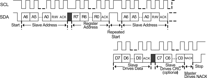
Figure 8-4 shows a read transaction using a Repeated Start.
 Figure 8-4 I2C Read with Repeated Start
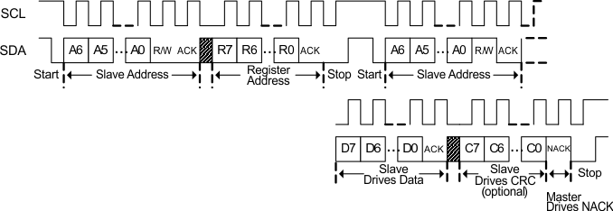
Figure 8-5 shows a read transaction where a Repeated Start is not used, for example if not available in hardware. For a block read, the master ACK’s each data byte except the last and continues to clock the interface. The I2C block will auto-increment the register address after each data byte.
When enabled, the CRC for a read transaction is calculated as follows:
- In a single-byte read transaction, the CRC is calculated after the second start and uses the slave address and data byte.
- In a block read transaction, the CRC for the first data byte is calculated after the second start and uses the slave address and data byte. The CRC for subsequent data bytes is calculated over the data byte only.
The CRC polynomial is x8 + x2 + x + 1, and the initial value is 0.
When the master detects a bad CRC, the I2C master will NACK the CRC, which causes the I2C slave to go to an idle state.
 Figure 8-5 I2C Read Without Repeated Start