ZHCSJU4I November 2006 – September 2018 CC1020
PRODUCTION DATA.
- 1器件概述
- 2修订历史记录
- 3Terminal Configuration and Functions
-
4Specifications
- 4.1 Absolute Maximum Ratings
- 4.2 ESD Ratings
- 4.3 Recommended Operating Conditions
- 4.4 RF Transmit
- 4.5 RF Receive
- 4.6 RSSI / Carrier Sense
- 4.7 Intermediate Frequency (IF)
- 4.8 Crystal Oscillator
- 4.9 Frequency Synthesizer
- 4.10 Digital Inputs and Outputs
- 4.11 Current Consumption
- 4.12 Thermal Resistance Characteristics for VQFNP Package
-
5Detailed Description
- 5.1 Overview
- 5.2 Functional Block Diagram
- 5.3 Configuration Overview
- 5.4 Microcontroller Interface
- 5.5 4-wire Serial Configuration Interface
- 5.6 Signal Interface
- 5.7 Data Rate Programming
- 5.8 Frequency Programming
- 5.9
Receiver
- 5.9.1 IF Frequency
- 5.9.2 Receiver Channel Filter Bandwidth
- 5.9.3 Demodulator, Bit Synchronizer, and Data Decision
- 5.9.4 Receiver Sensitivity Versus Data Rate and Frequency Separation
- 5.9.5 RSSI
- 5.9.6 Image Rejection Calibration
- 5.9.7 Blocking and Selectivity
- 5.9.8 Linear IF Chain and AGC Settings
- 5.9.9 AGC Settling
- 5.9.10 Preamble Length and Sync Word
- 5.9.11 Carrier Sense
- 5.9.12 Automatic Power-up Sequencing
- 5.9.13 Automatic Frequency Control
- 5.9.14 Digital FM
- 5.10 Transmitter
- 5.11 Input and Output Matching and Filtering
- 5.12 Frequency Synthesizer
- 5.13 VCO and LNA Current Control
- 5.14 Power Management
- 5.15 On-Off Keying (OOK)
- 5.16 Crystal Oscillator
- 5.17 Built-in Test Pattern Generator
- 5.18 Interrupt on Pin DCLK
- 5.19 PA_EN and LNA_EN Digital Output Pins
- 5.20 System Considerations and Guidelines
- 5.21 Antenna Considerations
- 5.22 Configuration Registers
- 6Applications, Implementation, and Layout
- 7器件和文档支持
- 8机械、封装和可订购信息
5.5 4-wire Serial Configuration Interface
The CC1020 device is configured via a simple 4-wire SPI-compatible interface (PDI, PDO, PCLK and PSEL) where the CC1020 device is the slave. There are 8-bit configuration registers, each addressed by a 7-bit address. A Read/Write bit initiates a read or write operation. A full configuration of the CC1020 device requires sending 33 data frames of 16 bits each (7 address bits, R/W bit and 8 data bits). The time needed for a full configuration depends on the PCLK frequency. With a PCLK frequency of 10 MHz the full configuration is done in less than 53 ms. Setting the device in power down mode requires sending one frame only and will in this case take less than 2 ms. All registers are also readable.
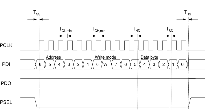
During each write-cycle, 16 bits are sent on the PDI-line. The seven most significant bits of each data frame (A6:0) are the address-bits. A6 is the MSB (Most Significant Bit) of the address and is sent as the first bit. The next bit is the R/W bit (high for write, low for read). The 8 data-bits are then transferred (D7:0). During address and data transfer the PSEL (Program Select) must be kept low. See Figure 5-4.
The timing for the programming is also shown in Figure 5-4 with reference to Table 5-1. The clocking of the data on PDI is done on the positive edge of PCLK. Data should be set up on the negative edge of PCLK by the microcontroller. When the last bit, D0, of the 8 data-bits has been loaded, the data word is loaded into the internal configuration register.
The configuration data will be retained during a programmed power down mode, but not when the power supply is turned off. The registers can be programmed in any order.
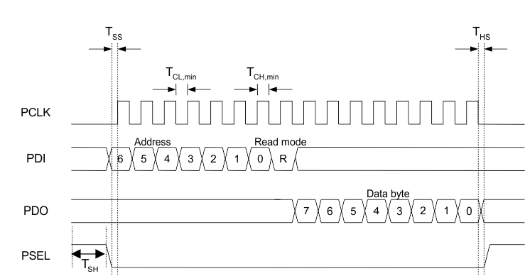
The configuration registers can also be read by the microcontroller via the same configuration interface. The seven address bits are sent first, then the R/W bit set low to initiate the data read-back. The CC1020 device then returns the data from the addressed register. PDO is used as the data output and must be configured as an input by the microcontroller. The PDO is set at the negative edge of PCLK and should be sampled at the positive edge. The read operation is illustrated in Figure 5-5.
PSEL must be set high between each read/write operation.
 Figure 5-4 Configuration Registers Write Operation
  Figure 5-5 Configuration Registers Read Operation
 Table 5-1 Serial Interface, Timing Specification(1)
| PARAMETER | MIN | MAX | UNIT | CONDITION | |
|---|---|---|---|---|---|
| FPCLK | PCLK, clock frequency | 10 | MHz | ||
| TCL,min | PCLK low pulse duration | 50 | ns | The minimum time PCLK must be low. | |
| TCH,min | PCLK high pulse duration | 50 | ns | The minimum time PCLK must be high. | |
| TSS | PSEL setup time | 25 | ns | The minimum time PSEL must be low before positive edge of PCLK. | |
| THS | PSEL hold time | 25 | ns | The minimum time PSEL must be held low after the negative edge of PCLK. | |
| TSH | PSEL high time | 50 | ns | The minimum time PSEL must be high. | |
| TSD | PDI setup time | 25 | ns | The minimum time data on PDI must be ready before the positive edge of PCLK. | |
| THD | PDI hold time | 25 | ns | The minimum time data must be held at PDI, after the positive edge of PCLK. | |
| Trise | Rise time | 100 | ns | The maximum rise time for PCLK and PSEL. | |
| Tfall | Fall time | 100 | ns | The maximum fall time for PCLK and PSEL. | |