ZHCSJU4I November 2006 – September 2018 CC1020
PRODUCTION DATA.
- 1器件概述
- 2修订历史记录
- 3Terminal Configuration and Functions
-
4Specifications
- 4.1 Absolute Maximum Ratings
- 4.2 ESD Ratings
- 4.3 Recommended Operating Conditions
- 4.4 RF Transmit
- 4.5 RF Receive
- 4.6 RSSI / Carrier Sense
- 4.7 Intermediate Frequency (IF)
- 4.8 Crystal Oscillator
- 4.9 Frequency Synthesizer
- 4.10 Digital Inputs and Outputs
- 4.11 Current Consumption
- 4.12 Thermal Resistance Characteristics for VQFNP Package
-
5Detailed Description
- 5.1 Overview
- 5.2 Functional Block Diagram
- 5.3 Configuration Overview
- 5.4 Microcontroller Interface
- 5.5 4-wire Serial Configuration Interface
- 5.6 Signal Interface
- 5.7 Data Rate Programming
- 5.8 Frequency Programming
- 5.9
Receiver
- 5.9.1 IF Frequency
- 5.9.2 Receiver Channel Filter Bandwidth
- 5.9.3 Demodulator, Bit Synchronizer, and Data Decision
- 5.9.4 Receiver Sensitivity Versus Data Rate and Frequency Separation
- 5.9.5 RSSI
- 5.9.6 Image Rejection Calibration
- 5.9.7 Blocking and Selectivity
- 5.9.8 Linear IF Chain and AGC Settings
- 5.9.9 AGC Settling
- 5.9.10 Preamble Length and Sync Word
- 5.9.11 Carrier Sense
- 5.9.12 Automatic Power-up Sequencing
- 5.9.13 Automatic Frequency Control
- 5.9.14 Digital FM
- 5.10 Transmitter
- 5.11 Input and Output Matching and Filtering
- 5.12 Frequency Synthesizer
- 5.13 VCO and LNA Current Control
- 5.14 Power Management
- 5.15 On-Off Keying (OOK)
- 5.16 Crystal Oscillator
- 5.17 Built-in Test Pattern Generator
- 5.18 Interrupt on Pin DCLK
- 5.19 PA_EN and LNA_EN Digital Output Pins
- 5.20 System Considerations and Guidelines
- 5.21 Antenna Considerations
- 5.22 Configuration Registers
- 6Applications, Implementation, and Layout
- 7器件和文档支持
- 8机械、封装和可订购信息
5.14 Power Management
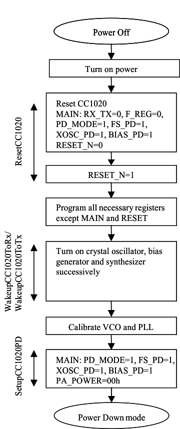
The CC1020 device offers great flexibility for power management in order to meet strict power consumption requirements in battery-operated applications. Power down mode is controlled through the MAIN register. There are separate bits to control the RX part, the TX part, the frequency synthesizer and the crystal oscillator in the MAIN register. This individual control can be used to optimize for lowest possible current consumption in each application. Figure 5-27 shows a typical power-on and initializing sequence for minimum power consumption.
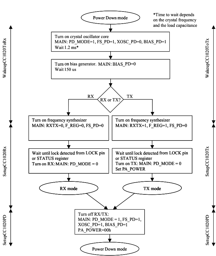
Figure 5-28 shows a typical sequence for activating RX and TX mode from power down mode for minimum power consumption.
NOTE
PSEL should be tri-stated or set to a high level during power down mode in order to prevent a trickle current from flowing in the internal pullup resistor.
Application Note AN023 CC1020 MCU Interfacing (SWRA069) includes example source code.
TI recommends resetting the CC1020 device (by clearing the RESET_N bit in the MAIN register) when the chip is powered up initially. All registers that need to be configured should then be programmed (those which differ from their default values). Registers can be programmed freely in any order. The CC1020 device should then be calibrated in both RX and TX mode. After this is completed, the CC1020 device is ready for use. See the detailed procedure flowcharts in Figure 5-26 through Figure 5-28.
With reference to Application Note AN023 CC1020 MCU Interfacing (SWRA069), TI recommends the following sequence:
After power up:
- ResetCC1020
- Initialize
- WakeUpCC1020ToRX
- Calibrate
- WakeUpCC1020ToTX
- Calibrate
After calibration is completed, enter TX mode (SetupCC1020TX), RX mode (SetupCC1020RX) or power down mode (SetupCC1020PD).
From power-down mode to RX:
- WakeUpCC1020ToRX
- SetupCC1020RX
From power-down mode to TX:
- WakeUpCC1020ToTX
- SetupCC1020TX
Switching from RX to TX mode:
- SetupCC1020TX
Switching from TX to RX mode:
- SetupCC1020RX
 Figure 5-27 Initializing Sequence
  Figure 5-28 Sequence for Activating RX or TX Mode