ZHCSJU4I November   2006  – September 2018 CC1020

PRODUCTION DATA.  

  1. 1器件概述
    1. 1.1 特性
    2. 1.2 应用
    3. 1.3 说明
    4. 1.4 功能方框图
  2. 2修订历史记录
  3. 3Terminal Configuration and Functions
    1. 3.1 Pin Diagram
    2. 3.2 Pin Configuration
  4. 4Specifications
    1. 4.1  Absolute Maximum Ratings
    2. 4.2  ESD Ratings
    3. 4.3  Recommended Operating Conditions
    4. 4.4  RF Transmit
    5. 4.5  RF Receive
    6. 4.6  RSSI / Carrier Sense
    7. 4.7  Intermediate Frequency (IF)
    8. 4.8  Crystal Oscillator
    9. 4.9  Frequency Synthesizer
    10. 4.10 Digital Inputs and Outputs
    11. 4.11 Current Consumption
    12. 4.12 Thermal Resistance Characteristics for VQFNP Package
  5. 5Detailed Description
    1. 5.1  Overview
    2. 5.2  Functional Block Diagram
    3. 5.3  Configuration Overview
      1. 5.3.1 Configuration Software
    4. 5.4  Microcontroller Interface
      1. 5.4.1 Configuration Interface
      2. 5.4.2 Signal Interface
      3. 5.4.3 PLL Lock Signal
    5. 5.5  4-wire Serial Configuration Interface
    6. 5.6  Signal Interface
      1. 5.6.1 Synchronous NRZ Mode
      2. 5.6.2 Transparent Asynchronous UART Mode
      3. 5.6.3 Synchronous Manchester Encoded Mode
        1. 5.6.3.1 Manchester Encoding and Decoding
    7. 5.7  Data Rate Programming
    8. 5.8  Frequency Programming
      1. 5.8.1 Dithering
    9. 5.9  Receiver
      1. 5.9.1  IF Frequency
      2. 5.9.2  Receiver Channel Filter Bandwidth
      3. 5.9.3  Demodulator, Bit Synchronizer, and Data Decision
      4. 5.9.4  Receiver Sensitivity Versus Data Rate and Frequency Separation
      5. 5.9.5  RSSI
      6. 5.9.6  Image Rejection Calibration
      7. 5.9.7  Blocking and Selectivity
      8. 5.9.8  Linear IF Chain and AGC Settings
      9. 5.9.9  AGC Settling
      10. 5.9.10 Preamble Length and Sync Word
      11. 5.9.11 Carrier Sense
      12. 5.9.12 Automatic Power-up Sequencing
      13. 5.9.13 Automatic Frequency Control
      14. 5.9.14 Digital FM
    10. 5.10 Transmitter
      1. 5.10.1 FSK Modulation Formats
      2. 5.10.2 Output Power Programming
      3. 5.10.3 TX Data Latency
      4. 5.10.4 Reducing Spurious Emission and Modulation Bandwidth
    11. 5.11 Input and Output Matching and Filtering
    12. 5.12 Frequency Synthesizer
      1. 5.12.1 VCO, Charge Pump and PLL Loop Filter
      2. 5.12.2 VCO and PLL Self-Calibration
      3. 5.12.3 PLL Turn-on Time Versus Loop Filter Bandwidth
      4. 5.12.4 PLL Lock Time Versus Loop Filter Bandwidth
    13. 5.13 VCO and LNA Current Control
    14. 5.14 Power Management
    15. 5.15 On-Off Keying (OOK)
    16. 5.16 Crystal Oscillator
    17. 5.17 Built-in Test Pattern Generator
    18. 5.18 Interrupt on Pin DCLK
      1. 5.18.1 Interrupt Upon PLL Lock
      2. 5.18.2 Interrupt Upon Received Signal Carrier Sense
    19. 5.19 PA_EN and LNA_EN Digital Output Pins
      1. 5.19.1 Interfacing an External LNA or PA
      2. 5.19.2 General Purpose Output Control Pins
      3. 5.19.3 PA_EN and LNA_EN Pin Drive
    20. 5.20 System Considerations and Guidelines
      1. 5.20.1 SRD Regulations
      2. 5.20.2 Narrowband Systems
      3. 5.20.3 Low Cost Systems
      4. 5.20.4 Battery Operated Systems
      5. 5.20.5 High Reliability Systems
      6. 5.20.6 Frequency Hopping Spread Spectrum Systems (FHSS)
    21. 5.21 Antenna Considerations
    22. 5.22 Configuration Registers
      1. 5.22.1 Memory
  6. 6Applications, Implementation, and Layout
    1. 6.1 Application Information
      1. 6.1.1 Typical Application
    2. 6.2 Design Requirements
      1. 6.2.1 Input and Output Matching
      2. 6.2.2 Bias Resistor
      3. 6.2.3 PLL Loop Filter
      4. 6.2.4 Crystal
      5. 6.2.5 Additional Filtering
      6. 6.2.6 Power Supply Decoupling and Filtering
    3. 6.3 PCB Layout Recommendations
  7. 7器件和文档支持
    1. 7.1 器件支持
      1. 7.1.1 器件命名规则
    2. 7.2 文档支持
      1. 7.2.1 Community Resources
    3. 7.3 商标
    4. 7.4 静电放电警告
    5. 7.5 Export Control Notice
    6. 7.6 Glossary
  8. 8机械、封装和可订购信息
    1. 8.1 封装信息

封装选项

机械数据 (封装 | 引脚)
散热焊盘机械数据 (封装 | 引脚)
订购信息

PA_EN and LNA_EN Pin Drive

Figure 5-32 shows the PA_EN and LNA_EN pin drive currents. The sink and source currents have opposite signs but absolute values are used in Figure 5-32.
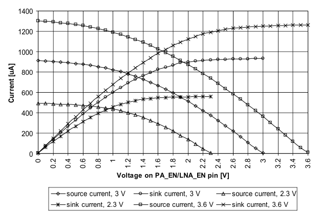
CC1020 typ_pa_en_lna_en_pin_Drv_swrs046.gifFigure 5-32 Typical PA_EN and LNA_EN Pin Drive