SWRS045F January 2006 – November 2018 CC1021
PRODUCTION DATA.
- 1Device Overview
- 2Revision History
- 3Terminal Configuration and Functions
-
4Specifications
- 4.1 Absolute Maximum Ratings
- 4.2 ESD Ratings
- 4.3 Recommended Operating Conditions
- 4.4 RF Transmit
- 4.5 RF Receive
- 4.6 RSSI / Carrier Sense
- 4.7 Intermediate Frequency (IF)
- 4.8 Crystal Oscillator
- 4.9 Frequency Synthesizer
- 4.10 Digital Inputs / Outputs
- 4.11 Current Consumption
- 4.12 Thermal Resistance Characteristics for VQFNP Package
-
5Detailed Description
- 5.1 Overview
- 5.2 Functional Block Diagram
- 5.3 Configuration Overview
- 5.4 Microcontroller Interface
- 5.5 4-wire Serial Configuration Interface
- 5.6 Signal Interface
- 5.7 Data Rate Programming
- 5.8 Frequency Programming
- 5.9
Receiver
- 5.9.1 IF Frequency
- 5.9.2 Receiver Channel Filter Bandwidth
- 5.9.3 Demodulator, Bit Synchronizer and Data Decision
- 5.9.4 Receiver Sensitivity versus Data Rate and Frequency Separation
- 5.9.5 RSSI
- 5.9.6 Image Rejection Calibration
- 5.9.7 Blocking and Selectivity
- 5.9.8 Linear IF Chain and AGC Settings
- 5.9.9 AGC Settling
- 5.9.10 Preamble Length and Sync Word
- 5.9.11 Carrier Sense
- 5.9.12 Automatic Power-Up Sequencing
- 5.9.13 Automatic Frequency Control
- 5.9.14 Digital FM
- 5.10 Transmitter
- 5.11 Input and Output Matching and Filtering
- 5.12 Frequency Synthesizer
- 5.13 VCO and LNA Current Control
- 5.14 Power Management
- 5.15 On-Off Keying (OOK)
- 5.16 Crystal Oscillator
- 5.17 Built-in Test Pattern Generator
- 5.18 Interrupt on Pin DCLK
- 5.19 PA_EN and LNA_EN Digital Output Pins
- 5.20 System Considerations and Guidelines
- 5.21 Antenna Considerations
- 5.22 Configuration Registers
- 6Applications, Implementation, and Layout
- 7Device and Documentation Support
- 8Mechanical Packaging and Orderable Information
5.11 Input and Output Matching and Filtering
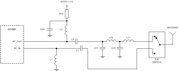
When designing the impedance matching network for the CC1021 device, the circuit must be matched correctly at the harmonic frequencies as well as at the fundamental tone. A recommended matching network is shown in Figure 5-22. Component values for various frequencies are given in Table 5-8. Component values for other frequencies can be found using the SmartRF™ Studio software.
As can be seen from Figure 5-22 and Table 5-8, the 433 MHz network utilizes a T-type filter, while the 868/915 MHz network has a π-type filter topology.
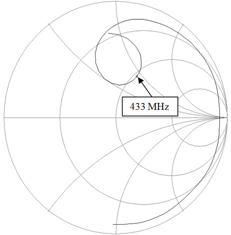
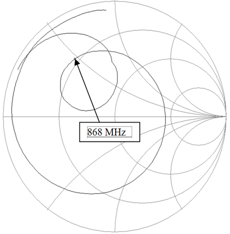
It is important to remember that the physical layout and the components used contribute significantly to the reflection coefficient, especially at the higher harmonics. For this reason, the frequency response of the matching network should be measured and compared to the response of the TI reference design. Refer to Figure 5-24 and Table 5-9 as well as Figure 5-25 and Table 5-10.
The use of an external T/R switch reduces current consumption in TX for high output power levels and improves the sensitivity in RX. A recommended application circuit is available from the TI web site (CC1020EMX). The external T/R switch can be omitted in certain applications, but performance will then be degraded.
The match can also be tuned by a shunt capacitor array at the PA output (RF_OUT). The capacitance can be set in 0.4 pF steps and used either in RX mode or TX mode. The RX_MATCH[3:0] and TX_MATCH[3:0] bits in the MATCH register control the capacitor array.
Table 5-8 Component Values for the Matching Network Described in Figure 5-22
| ITEM | 433 MHz | 868 MHz | 915 MHz |
|---|---|---|---|
| C1 | 10 pF, 5%, NP0, 0402 | 47 pF, 5%, NP0, 0402 | 47 pF, 5%, NP0, 0402 |
| C3 | 5.6 pF, 5%, NP0, 0402 | 10 pF, 5%, NP0, 0402 | 10 pF, 5%, NP0, 0402 |
| C60 | 220 pF, 5%, NP0, 0402 | 220 pF, 5%, NP0, 0402 | 220 pF, 5%, NP0, 0402 |
| C71 | DNM(1) | 8.2 pF 5%, NP0, 0402 | 8.2 pF 5%, NP0, 0402 |
| C72 | 4.7 pF, 5%, NP0, 0402 | 8.2 pF 5%, NP0, 0402 | 8.2 pF 5%, NP0, 0402 |
| L1 | 33 nH, 5%, 0402 | 82 nH, 5%, 0402 | 82 nH, 5%, 0402 |
| L2 | 22 nH, 5%, 0402 | 3.6 nH, 5%, 0402 | 3.6 nH, 5%, 0402 |
| L70 | 47 nH, 5%, 0402 | 5.1 nH, 5%, 0402 | 5.1 nH, 5%, 0402 |
| L71 | 39 nH, 5%, 0402 | 0 Ω resistor, 0402 | 0 Ω resistor, 0402 |
| R10 | 82 Ω, 5%, 0402 | 82 Ω, 5%, 0402 | 82 Ω, 5%, 0402 |
 Figure 5-22 Input and Output Matching Network
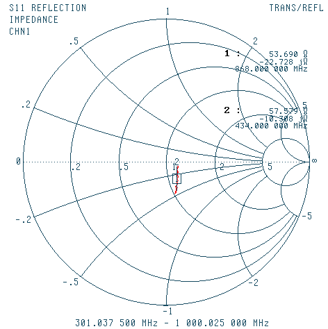
  Figure 5-23 Typical LNA Input Impedance, 200 to 1000 MHz
  Figure 5-24 Typical Optimum PA Load Impedance, 433 MHz.
The frequency is swept from 300 MHz to 2500 MHz.
Values are listed in Table 5-9
Table 5-9 Impedances at the First 5 Harmonics (433 MHz Matching Network)
| FREQUENCY
(MHz) |
REAL
(Ohms) |
IMAGINARY
(Ohms) |
|---|---|---|
| 433 | 54 | 44 |
| 866 | 20 | 173 |
| 1299 | 288 | –563 |
| 1732 | 14 | –123 |
| 2165 | 5 | –66 |
 Figure 5-25 Typical Optimum PA Load Impedance, 868/915 MHz.
The frequency is swept from 300 MHz to 2800 MHz.
Values are listed in Table 5-10
Table 5-10 Impedances at the First 3 Harmonics
(868/915 MHz Matching Network)
| FREQUENCY
(MHz) |
REAL
(Ohms) |
IMAGINARY
(Ohms) |
|---|---|---|
| 868 | 15 | 24 |
| 915 | 20 | 35 |
| 1736 | 1.5 | 18 |
| 1830 | 1.7 | 22 |
| 2604 | 3.2 | 44 |
| 2745 | 3.6 | 45 |