SWRS045F January 2006 – November 2018 CC1021
PRODUCTION DATA.
- 1Device Overview
- 2Revision History
- 3Terminal Configuration and Functions
-
4Specifications
- 4.1 Absolute Maximum Ratings
- 4.2 ESD Ratings
- 4.3 Recommended Operating Conditions
- 4.4 RF Transmit
- 4.5 RF Receive
- 4.6 RSSI / Carrier Sense
- 4.7 Intermediate Frequency (IF)
- 4.8 Crystal Oscillator
- 4.9 Frequency Synthesizer
- 4.10 Digital Inputs / Outputs
- 4.11 Current Consumption
- 4.12 Thermal Resistance Characteristics for VQFNP Package
-
5Detailed Description
- 5.1 Overview
- 5.2 Functional Block Diagram
- 5.3 Configuration Overview
- 5.4 Microcontroller Interface
- 5.5 4-wire Serial Configuration Interface
- 5.6 Signal Interface
- 5.7 Data Rate Programming
- 5.8 Frequency Programming
- 5.9
Receiver
- 5.9.1 IF Frequency
- 5.9.2 Receiver Channel Filter Bandwidth
- 5.9.3 Demodulator, Bit Synchronizer and Data Decision
- 5.9.4 Receiver Sensitivity versus Data Rate and Frequency Separation
- 5.9.5 RSSI
- 5.9.6 Image Rejection Calibration
- 5.9.7 Blocking and Selectivity
- 5.9.8 Linear IF Chain and AGC Settings
- 5.9.9 AGC Settling
- 5.9.10 Preamble Length and Sync Word
- 5.9.11 Carrier Sense
- 5.9.12 Automatic Power-Up Sequencing
- 5.9.13 Automatic Frequency Control
- 5.9.14 Digital FM
- 5.10 Transmitter
- 5.11 Input and Output Matching and Filtering
- 5.12 Frequency Synthesizer
- 5.13 VCO and LNA Current Control
- 5.14 Power Management
- 5.15 On-Off Keying (OOK)
- 5.16 Crystal Oscillator
- 5.17 Built-in Test Pattern Generator
- 5.18 Interrupt on Pin DCLK
- 5.19 PA_EN and LNA_EN Digital Output Pins
- 5.20 System Considerations and Guidelines
- 5.21 Antenna Considerations
- 5.22 Configuration Registers
- 6Applications, Implementation, and Layout
- 7Device and Documentation Support
- 8Mechanical Packaging and Orderable Information
5.9.8 Linear IF Chain and AGC Settings
The CC1021 device is based on a linear IF chain where the signal amplification is done in an analog VGA (Variable Gain Amplifier). The gain is controlled by the digital part of the IF chain after the ADC (Analog to Digital Converter). The AGC (Automatic Gain Control) loop ensures that the ADC operates inside its dynamic range by using an analog/digital feedback loop.
The maximum VGA gain is programmed by the VGA_SETTING[4:0] in the VGA3 register. The VGA gain is programmed in approximately 3 dB/LSB. The VGA gain should be set so that the amplified thermal noise from the front-end balance the quantization noise from the ADC. Therefore the optimum maximum VGA gain setting will depend on the channel filter bandwidth.
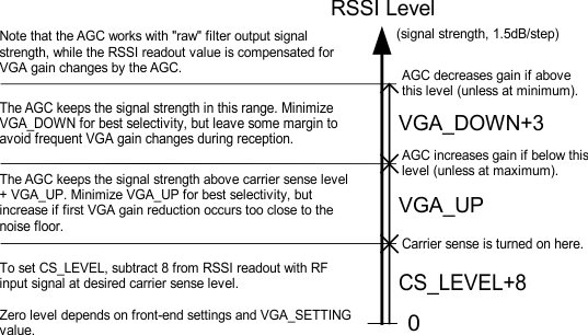
A digital RSSI is used to measure the signal strength after the ADC. The CS_LEVEL[4:0] in the VGA4 register is used to set the nominal operating point of the gain control (and also the carrier sense level). Further explanation can be found in Figure 5-17.
The VGA gain will be changed according to a threshold set by the VGA_DOWN[2:0] in the VGA3 register and the VGA_UP[2:0] in the VGA4 register. Together, these two values specify the signal strength limits used by the AGC to adjust the VGA gain.
To avoid unnecessary tripping of the VGA, an extra hysteresis and filtering of the RSSI samples can be added. The AGC_HYSTERESIS bit in the VGA2 register enables this.
The time dynamics of the loop can be altered by the VGA_BLANKING bit in the ANALOG register, and VGA_FREEZE[1:0] and VGA_WAIT[2:0] bits in the VGA1 register.
When VGA_BLANKING is activated, the VGA recovery time from DC offset spikes after a gain step is reduced.
VGA_FREEZE determines the time to hold bit synchronization, VGA and RSSI levels after one of these events occur:
- RX power-up
- The PLL has been out of lock
- Frequency register setting is switched between A and B
This feature is useful to avoid AGC operation during start-up transients and to ensure minimum dwell time using frequency hopping. This means that bit synchronization can be maintained from hop to hop.
VGA_WAIT determines the time to hold the present bit synchronization and RSSI levels after changing VGA gain. This feature is useful to avoid AGC operation during the settling of transients after a VGA gain change. Some transients are expected due to DC offsets in the VGA.
At the sensitivity limit, the VGA gain is set by VGA_SETTING. In order to optimize selectivity, this gain should not be set higher than necessary. The SmartRF™ Studio software gives the settings for VGA1 through VGA4 registers. For reference, the following method can be used to find the AGC settings:
- Disable AGC and use maximum LNA2 gain by writing BFh to the VGA2 register. Set minimum VGA gain by writing to the VGA3 register with VGA_SETTING = 0.
- Apply no RF input signal, and measure ADC noise floor by reading the RSSI register.
- Apply no RF input signal, and write VGA3 register with increasing VGA_SETTING value until the RSSI register value is approximately 4 larger than the value read in step 2. This places the front-end noise floor around 6 dB above the ADC noise floor.
- Apply an RF signal with strength equal the desired carrier sense threshold. The RF signal should preferably be modulated with correct Baud rate and deviation. Read the RSSI register value, subtract 8, and write to CS_LEVEL in the VGA4 register. Vary the RF signal level slightly and check that carrier sense indication (bit 3 in STATUS register) switches at the desired input level.
- If desired, adjust the VGA_UP and VGA_DOWN settings according to the explanation in Figure 5-17.
- Enable AGC and select LNA2 gain change level. Write 55h to VGA2 register if the resulting VGA_SETTING>10. Otherwise, write 45h to VGA2. Modify AGC_AVG in the above VGA2 value if faster carrier sense and AGC settling is desired.
 Figure 5-17 Relationship Between RSSI, Carrier Sense Level,
and AGC Settings CS_LEVEL, VGA_UP and VGA_DOWN