ZHCSQ71 March 2022 CC1311P3
PRODUCTION DATA
- 1 特性
- 2 应用
- 3 说明
- 4 功能方框图
- 5 Revision History
- 6 Device Comparison
- 7 Pin Configuration and Functions
-
8 Specifications
- 8.1 Absolute Maximum Ratings
- 8.2 ESD Ratings
- 8.3 Recommended Operating Conditions
- 8.4 Power Supply and Modules
- 8.5 Power Consumption - Power Modes
- 8.6 Power Consumption - Radio Modes
- 8.7 Nonvolatile (Flash) Memory Characteristics
- 8.8 Thermal Resistance Characteristics
- 8.9 RF Frequency Bands
- 8.10 861 MHz to 1054 MHz - Receive (RX)
- 8.11 861 MHz to 1054 MHz - Transmit (TX)
- 8.12 861 MHz to 1054 MHz - PLL Phase Noise Wideband Mode
- 8.13 861 MHz to 1054 MHz - PLL Phase Noise Narrowband Mode
- 8.14 359 MHz to 527 MHz - Receive (RX)
- 8.15 359 MHz to 527 MHz - Transmit (TX)
- 8.16 359 MHz to 527 MHz - PLL Phase Noise
- 8.17 Timing and Switching Characteristics
- 8.18 Peripheral Characteristics
- 8.19 Typical Characteristics
- 9 Detailed Description
- 10Application, Implementation, and Layout
- 11Device and Documentation Support
- 12Mechanical, Packaging, and Orderable Information
封装选项
请参考 PDF 数据表获取器件具体的封装图。
机械数据 (封装 | 引脚)
- RGZ|48
散热焊盘机械数据 (封装 | 引脚)
- RGZ|48
订购信息
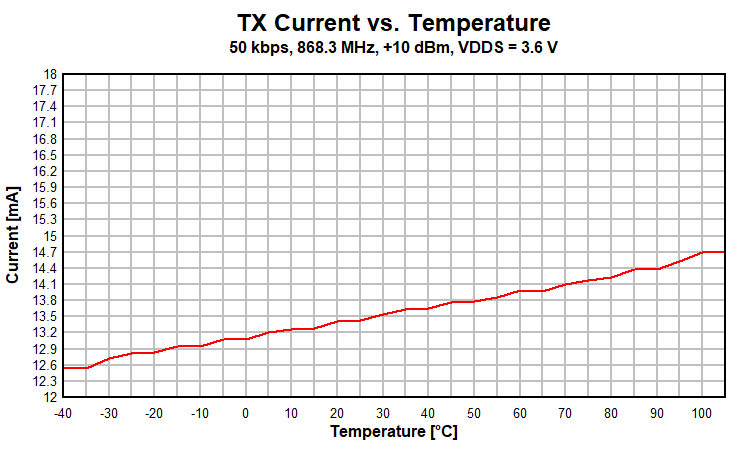
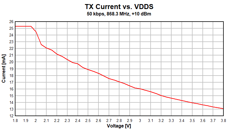
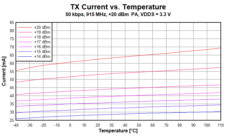
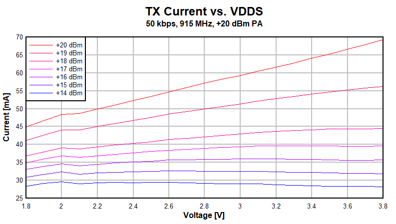
8.19.3 TX Current


Table 8-2 shows typical TX current and output power for different output power settings.
Table 8-1 Typical TX Current and Output
Power, high power PA (915 MHz, VDDS = 3.3 V)
| CC1311P3 at 915 MHz, VDDS = 3.3 V (Measured on CC1311-P3EM-7XD7793-PA915) | |||
|---|---|---|---|
| txPower | TX Power Setting (SmartRF Studio) | Typical Output Power [dBm] | Typical Current Consumption [mA] |
| 0x1B8ED2 | 20 | 20.6 | 64.9 |
| 0x448CF | 19 | 19.5 | 55.4 |
| 0x48022 | 18 | 18.0 | 46.0 |
| 0x2661C | 17 | 17.1 | 41.5 |
| 0x5618 | 16 | 16.2 | 37.6 |
| 0x4812 | 15 | 15.2 | 33.9 |
| 0x380D | 14 | 14.0 | 30.2 |
Table 8-2 Typical TX Current and Output
Power (868 MHz, VDDS = 3.0 V)
| CC1311P3 at 868 MHz, VDDS = 3.0 V (Measured on CC1311-P3EM-7XD7793-PA915) | |||
|---|---|---|---|
| txPower | TX Power Setting (SmartRF Studio) | Typical Output Power [dBm] | Typical Current Consumption [mA] |
| 0x013F(1) | 14 | 13.8 | 30.0 |
| 0xB224 | 12.5 | 12.2 | 21.5 |
| 0x895E | 12 | 11.8 | 20.3 |
| 0x669A | 11 | 10.8 | 18.1 |
| 0x3E92 | 10 | 9.8 | 16.4 |
| 0x3EDC | 9 | 8.9 | 15.5 |
| 0x2CD8 | 8 | 8.1 | 14.5 |
| 0x26D4 | 7 | 7.0 | 13.3 |
| 0x20D1 | 6 | 5.8 | 12.2 |
| 0x1CCE | 5 | 4.4 | 10.9 |
| 0x16CD | 4 | 3.7 | 10.5 |
| 0x14CB | 3 | 2.2 | 9.7 |
| 0x12CA | 2 | 1.5 | 9.2 |
| 0x12C9 | 1 | 0.6 | 8.8 |
| 0x10C8 | 0 | -0.5 | 8.3 |
| 0xAC4 | -5 | -7.3 | 6.5 |
| 0xAC2 | -10 | -13.1 | 5.6 |
| 0x6C1 | -15 | -18.3 | 5.2 |
| 0x4C0 | -20 | -22.6 | 4.9 |
1. Boost mode enabled. VDDR regulated to 1.95
V.