ZHCSHI1H january   2018  – november 2020 CC1312R

PRODUCTION DATA  

  1. 特性
  2. 应用
  3. 说明
  4. Functional Block Diagram
  5. Revision History
  6. Device Comparison
  7. Terminal Configuration and Functions
    1. 7.1 Pin Diagram – RGZ Package (Top View)
    2. 7.2 Signal Descriptions – RGZ Package
    3. 7.3 Connections for Unused Pins and Modules
  8. Specifications
    1. 8.1  Absolute Maximum Ratings
    2. 8.2  ESD Ratings
    3. 8.3  Recommended Operating Conditions
    4. 8.4  Power Supply and Modules
    5. 8.5  Power Consumption - Power Modes
    6. 8.6  Power Consumption - Radio Modes
    7. 8.7  Nonvolatile (Flash) Memory Characteristics
    8. 8.8  Thermal Resistance Characteristics
    9. 8.9  RF Frequency Bands
    10. 8.10 861 MHz to 1054 MHz - Receive (RX)
    11. 8.11 861 MHz to 1054 MHz - Transmit (TX) 
    12. 8.12 861 MHz to 1054 MHz - PLL Phase Noise Wideband Mode
    13. 8.13 861 MHz to 1054 MHz - PLL Phase Noise Narrowband Mode
    14. 8.14 359 MHz to 527 MHz - Receive (RX)
    15. 8.15 359 MHz to 527 MHz - Transmit (TX) 
    16. 8.16 359 MHz to 527 MHz - PLL Phase Noise
    17. 8.17 143 MHz to 176 MHz - Receive (RX)
    18. 8.18 143 MHz to 176 MHz  - Transmit (TX) 
    19. 8.19 143 MHz to 176 MHz - PLL Phase Noise
    20. 8.20 Timing and Switching Characteristics
      1. 8.20.1 Reset Timing
      2. 8.20.2 Wakeup Timing
      3. 8.20.3 Clock Specifications
        1. 8.20.3.1 48 MHz Clock Input (TCXO)
        2. 8.20.3.2 48 MHz Crystal Oscillator (XOSC_HF)
        3. 8.20.3.3 48 MHz RC Oscillator (RCOSC_HF)
        4. 8.20.3.4 2 MHz RC Oscillator (RCOSC_MF)
        5. 8.20.3.5 32.768 kHz Crystal Oscillator (XOSC_LF)
        6. 8.20.3.6 32 kHz RC Oscillator (RCOSC_LF)
      4. 8.20.4 Synchronous Serial Interface (SSI) Characteristics
        1. 8.20.4.1 Synchronous Serial Interface (SSI) Characteristics
        2.       43
      5. 8.20.5 UART
        1. 8.20.5.1 UART Characteristics
    21. 8.21 Peripheral Characteristics
      1. 8.21.1 ADC
        1. 8.21.1.1 Analog-to-Digital Converter (ADC) Characteristics
      2. 8.21.2 DAC
        1. 8.21.2.1 Digital-to-Analog Converter (DAC) Characteristics
      3. 8.21.3 Temperature and Battery Monitor
        1. 8.21.3.1 Temperature Sensor
        2. 8.21.3.2 Battery Monitor
      4. 8.21.4 Comparators
        1. 8.21.4.1 Low-Power Clocked Comparator
        2. 8.21.4.2 Continuous Time Comparator
      5. 8.21.5 Current Source
        1. 8.21.5.1 Programmable Current Source
      6. 8.21.6 GPIO
        1. 8.21.6.1 GPIO DC Characteristics
    22. 8.22 Typical Characteristics
      1. 8.22.1 MCU Current
      2. 8.22.2 RX Current
      3. 8.22.3 TX Current
      4. 8.22.4 RX Performance
      5. 8.22.5 TX Performance
      6. 8.22.6 ADC Performance
  9. Detailed Description
    1. 9.1  Overview
    2. 9.2  System CPU
    3. 9.3  Radio (RF Core)
      1. 9.3.1 Proprietary Radio Formats
    4. 9.4  Memory
    5. 9.5  Sensor Controller
    6. 9.6  Cryptography
    7. 9.7  Timers
    8. 9.8  Serial Peripherals and I/O
    9. 9.9  Battery and Temperature Monitor
    10. 9.10 µDMA
    11. 9.11 Debug
    12. 9.12 Power Management
    13. 9.13 Clock Systems
    14. 9.14 Network Processor
  10. 10Application, Implementation, and Layout
    1. 10.1 Reference Designs
    2. 10.2 Junction Temperature Calculation
  11. 11Device and Documentation Support
    1. 11.1 Tools and Software
      1. 11.1.1 SimpleLink™ Microcontroller Platform
    2. 11.2 Documentation Support
    3. 11.3 支持资源
    4. 11.4 Trademarks
    5. 11.5 静电放电警告
    6. 11.6 术语表
  12. 12Mechanical, Packaging, and Orderable Information
    1. 12.1 Packaging Information

封装选项

请参考 PDF 数据表获取器件具体的封装图。

机械数据 (封装 | 引脚)
  • RGZ|48
散热焊盘机械数据 (封装 | 引脚)
订购信息

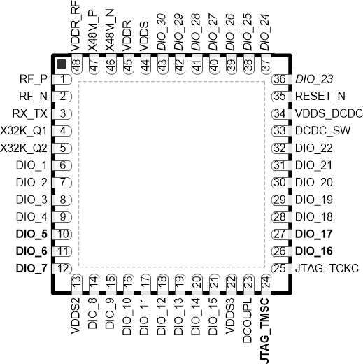
Pin Diagram – RGZ Package (Top View)

GUID-794F08F9-1B19-4C05-B46B-0F879833E9C7-low.gifFigure 7-1 RGZ (7-mm × 7-mm) Pinout, 0.5-mm Pitch (Top View)


The following I/O pins marked in Figure 7-1 in bold have high-drive capabilities:

  • Pin 10, DIO_5
  • Pin 11, DIO_6
  • Pin 12, DIO_7
  • Pin 24, JTAG_TMSC
  • Pin 26, DIO_16
  • Pin 27, DIO_17

The following I/O pins marked in Figure 7-1 in italics have analog capabilities:

  • Pin 36, DIO_23
  • Pin 37, DIO_24
  • Pin 38, DIO_25
  • Pin 39, DIO_26
  • Pin 40, DIO_27
  • Pin 41, DIO_28
  • Pin 42, DIO_29
  • Pin 43, DIO_30