ZHCSFW7C
december 2016 – september 2020
CC2640R2F
PRODUCTION DATA
1
特性
2
应用
3
说明
4
Functional Block Diagram
5
Revision History
6
Device Comparison
6.1
Related Products
7
Terminal Configuration and Functions
7.1
Pin Diagram – RGZ Package
7.2
Signal Descriptions – RGZ Package
7.3
Pin Diagram – RHB Package
7.4
Signal Descriptions – RHB Package
7.5
Pin Diagram – YFV (Chip Scale, DSBGA) Package
7.6
Signal Descriptions – YFV (Chip Scale, DSBGA) Package
7.7
Pin Diagram – RSM Package
7.8
Signal Descriptions – RSM Package
8
Specifications
8.1
Absolute Maximum Ratings
8.2
ESD Ratings
8.3
Recommended Operating Conditions
8.4
Power Consumption Summary
8.5
General Characteristics
8.6
125-kbps Coded (Bluetooth 5) – RX
8.7
125-kbps Coded (Bluetooth 5) – TX
8.8
500-kbps Coded (Bluetooth 5) – RX
8.9
500-kbps Coded (Bluetooth 5) – TX
8.10
1-Mbps GFSK (Bluetooth low energy) – RX
8.11
1-Mbps GFSK (Bluetooth low energy) – TX
8.12
2-Mbps GFSK (Bluetooth 5) – RX
8.13
2-Mbps GFSK (Bluetooth 5) – TX
8.14
24-MHz Crystal Oscillator (XOSC_HF)
8.15
32.768-kHz Crystal Oscillator (XOSC_LF)
8.16
48-MHz RC Oscillator (RCOSC_HF)
8.17
32-kHz RC Oscillator (RCOSC_LF)
8.18
ADC Characteristics
8.19
Temperature Sensor
8.20
Battery Monitor
8.21
Continuous Time Comparator
8.22
Low-Power Clocked Comparator
8.23
Programmable Current Source
8.24
Synchronous Serial Interface (SSI)
8.25
DC Characteristics
8.26
Thermal Resistance Characteristics
8.27
Timing Requirements
8.28
Switching Characteristics
8.29
Typical Characteristics
9
Detailed Description
9.1
Overview
9.2
Functional Block Diagram
9.3
Main CPU
9.4
RF Core
9.5
Sensor Controller
9.6
Memory
9.7
Debug
9.8
Power Management
9.9
Clock Systems
9.10
General Peripherals and Modules
9.11
Voltage Supply Domains
9.12
System Architecture
10
Application, Implementation, and Layout
10.1
Application Information
10.2
5 × 5 External Differential (5XD) Application Circuit
10.2.1
Layout
10.3
4 × 4 External Single-ended (4XS) Application Circuit
10.3.1
Layout
11
Device and Documentation Support
11.1
Device Nomenclature
11.2
Tools and Software
11.3
Documentation Support
11.4
Texas Instruments Low-Power RF Website
11.5
Low-Power RF eNewsletter
11.6
支持资源
11.7
Trademarks
11.8
静电放电警告
11.9
Export Control Notice
11.10
术语表
12
Mechanical, Packaging, and Orderable Information
12.1
Packaging Information
封装选项
请参考 PDF 数据表获取器件具体的封装图。
机械数据 (封装 | 引脚)
RSM|32
RGZ|48
RHB|32
YFV|34
散热焊盘机械数据 (封装 | 引脚)
RGZ|48
QFND031W
RSM|32
QFND112H
RHB|32
QFND029X
订购信息
zhcsfw7c_oa
zhcsfw7c_pm
8.29
Typical Characteristics
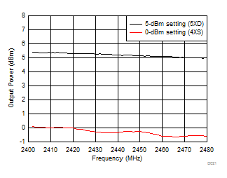
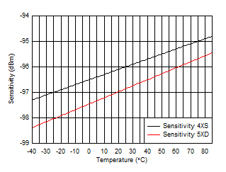
Figure 8-4
BLE Sensitivity vs Temperature
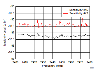
Figure 8-6
BLE Sensitivity vs Channel Frequency
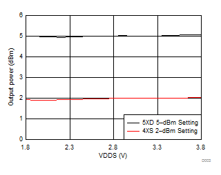
Figure 8-8
TX Output Power vs Supply Voltage (VDDS)
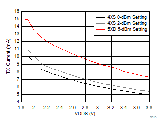
Figure 8-10
TX Current Consumption vs Supply Voltage (VDDS)
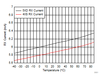
Figure 8-12
RX Mode Current Consumption vs Temperature
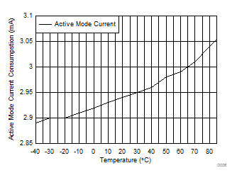
Figure 8-14
Active Mode (MCU Running, No Peripherals) Current Consumption vs Temperature
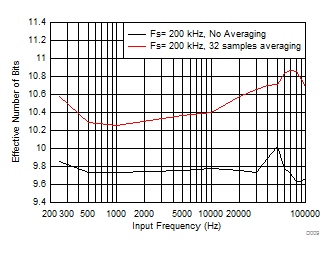
Figure 8-16
SoC ADC Effective Number of Bits vs Input Frequency (Internal Reference, Scaling enabled)
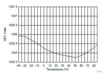
Figure 8-18
SoC ADC Output vs Temperature (Fixed Input, Internal Reference)
Figure 8-20
Standby Mode Supply Current vs Temperature
Figure 8-5
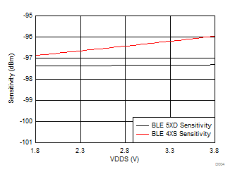
BLE Sensitivity vs Supply Voltage (VDDS)
Figure 8-7
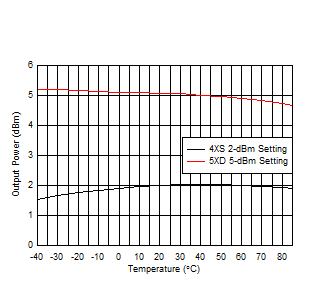
TX Output Power vs Temperature
Figure 8-9
TX Output Power vs Channel Frequency
Figure 8-11
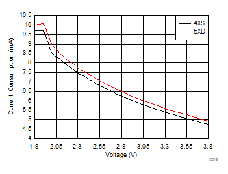
RX Mode Current vs Supply Voltage (VDDS)
Figure 8-13
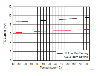
TX Mode Current Consumption vs Temperature
Figure 8-15
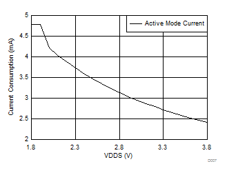
Active Mode (MCU Running, No Peripherals) Current Consumption vs Supply Voltage (VDDS)
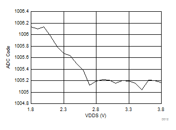
Figure 8-17
SoC ADC Output vs Supply Voltage (Fixed Input, Internal Reference)
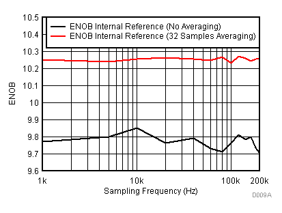
Figure 8-19
SoC ADC ENOB vs Sampling Frequency (Scaling enabled, input frequency = FS / 10)
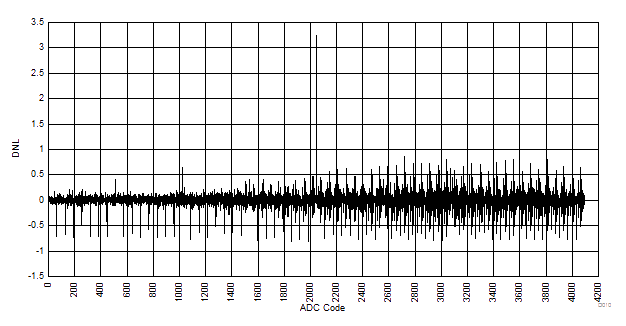
Figure 8-21
SoC ADC DNL vs ADC Code (Internal Reference)
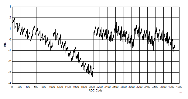
Figure 8-22
SoC ADC INL vs ADC Code (Internal Reference)
千亿体育app官网登录(中国)官方网站IOS/安卓通用版/手机APP
|
米乐app下载官网(中国)|ios|Android/通用版APP最新版
|
米乐|米乐·M6(中国大陆)官方网站
|
千亿体育登陆地址
|
华体会体育(中国)HTH·官方网站
|
千赢qy国际_全站最新版千赢qy国际V6.2.14安卓/IOS下载
|
18新利网v1.2.5|中国官方网站
|
bob电竞真人(中国官网)安卓/ios苹果/电脑版【1.97.95版下载】
|
千亿体育app官方下载(中国)官方网站IOS/安卓/手机APP下载安装
|