ZHCSSP3B December   2022  – April 2024 CC2674R10

PRODUCTION DATA  

  1.   1
  2. 特性
  3. 应用
  4. 说明
  5. 功能方框图
  6. Device Comparison
  7. Pin Configuration and Functions
    1. 6.1 Pin Diagram—RGZ Package (Top View)
    2. 6.2 Signal Descriptions—RGZ Package
    3. 6.3 Connections for Unused Pins and Modules—RGZ Package
    4. 6.4 Pin Diagram—RSK Package (Top View)
    5. 6.5 Signal Descriptions—RSK Package
    6. 6.6 Connection of Unused Pins and Module—RSK Package
  8. Specifications
    1. 7.1  Absolute Maximum Ratings
    2. 7.2  ESD Ratings
    3. 7.3  Recommended Operating Conditions
    4. 7.4  Power Supply and Modules
    5. 7.5  Power Consumption - Power Modes
    6. 7.6  Power Consumption - Radio Modes
    7. 7.7  Nonvolatile (Flash) Memory Characteristics
    8. 7.8  Thermal Resistance Characteristics
    9. 7.9  RF Frequency Bands
    10. 7.10 Bluetooth Low Energy—Receive (RX)
    11. 7.11 Bluetooth Low Energy—Transmit (TX)
    12. 7.12 Zigbee and Thread - IEEE 802.15.4-2006 2.4GHz (OQPSK DSSS1:8, 250kbps) - RX
    13. 7.13 Zigbee and Thread - IEEE 802.15.4-2006 2.4GHz (OQPSK DSSS1:8, 250kbps) - TX
    14. 7.14 Timing and Switching Characteristics
      1. 7.14.1 Reset Timing
      2. 7.14.2 Wakeup Timing
      3. 7.14.3 Clock Specifications
        1. 7.14.3.1 48MHz Crystal Oscillator (XOSC_HF)
        2. 7.14.3.2 48MHz RC Oscillator (RCOSC_HF)
        3. 7.14.3.3 2MHz RC Oscillator (RCOSC_MF)
        4. 7.14.3.4 32.768 kHz Crystal Oscillator (XOSC_LF)
        5. 7.14.3.5 32 kHz RC Oscillator (RCOSC_LF)
      4. 7.14.4 Serial Peripheral Interface (SPI) Characteristics
        1. 7.14.4.1 SPI Characteristics
        2. 7.14.4.2 SPI Master Mode
        3. 7.14.4.3 SPI Master Mode Timing Diagrams
        4. 7.14.4.4 SPI Slave Mode
        5. 7.14.4.5 SPI Slave Mode Timing Diagrams
      5. 7.14.5 UART
        1. 7.14.5.1 UART Characteristics
    15. 7.15 Peripheral Characteristics
      1. 7.15.1 ADC
        1. 7.15.1.1 Analog-to-Digital Converter (ADC) Characteristics
      2. 7.15.2 DAC
        1. 7.15.2.1 Digital-to-Analog Converter (DAC) Characteristics
      3. 7.15.3 Temperature and Battery Monitor
        1. 7.15.3.1 Temperature Sensor
        2. 7.15.3.2 Battery Monitor
      4. 7.15.4 Comparators
        1. 7.15.4.1 Low-Power Clocked Comparator
        2. 7.15.4.2 Continuous Time Comparator
      5. 7.15.5 Current Source
        1. 7.15.5.1 Programmable Current Source
      6. 7.15.6 GPIO
        1. 7.15.6.1 GPIO DC Characteristics
    16. 7.16 Typical Characteristics
      1. 7.16.1 MCU Current
      2. 7.16.2 RX Current
      3. 7.16.3 TX Current
      4. 7.16.4 RX Performance
      5. 7.16.5 TX Performance
      6. 7.16.6 ADC Performance
  9. Detailed Description
    1. 8.1  Overview
    2. 8.2  System CPU
    3. 8.3  Radio (RF Core)
      1. 8.3.1 Bluetooth 5.3 Low Energy
      2. 8.3.2 802.15.4 Thread, Zigbee, and 6LoWPAN
    4. 8.4  Memory
    5. 8.5  Sensor Controller
    6. 8.6  Cryptography
    7. 8.7  Timers
    8. 8.8  Serial Peripherals and I/O
    9. 8.9  Battery and Temperature Monitor
    10. 8.10 µDMA
    11. 8.11 Debug
    12. 8.12 Power Management
    13. 8.13 Clock Systems
    14. 8.14 Network Processor
  10. Application, Implementation, and Layout
    1. 9.1 Reference Designs
  11. 10Device and Documentation Support
    1. 10.1 Tools and Software
      1. 10.1.1 SimpleLink™ Microcontroller Platform
    2. 10.2 Documentation Support
    3. 10.3 支持资源
    4. 10.4 Trademarks
    5. 10.5 静电放电警告
    6. 10.6 术语表
  12. 11Revision History
  13. 12Mechanical, Packaging, and Orderable Information
    1. 12.1 Packaging Information

封装选项

机械数据 (封装 | 引脚)
散热焊盘机械数据 (封装 | 引脚)
订购信息

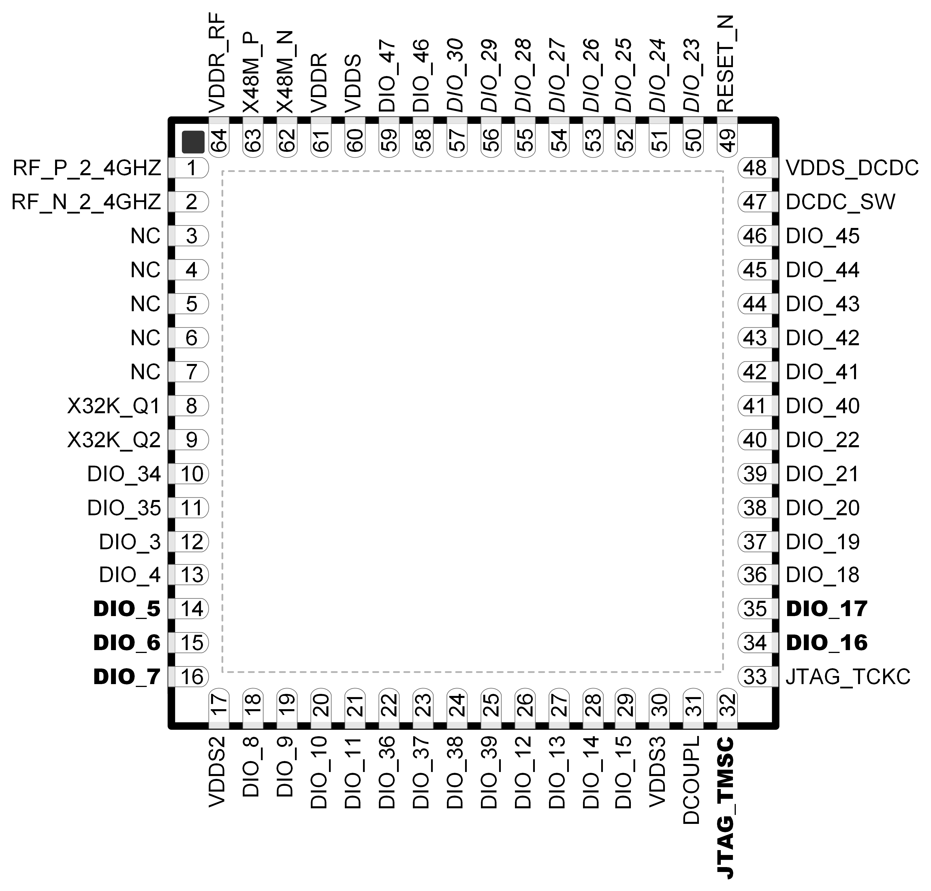
Pin Diagram—RSK Package (Top View)

CC2674R10 RSK
                    (8mm
                    ×
                    8mm)
                    Pinout,
                    0.4mm
                    Pitch (Top View) Figure 6-2 RSK (8mm × 8mm) Pinout, 0.4mm Pitch (Top View)

The following I/O pins marked in Figure 6-2 in bold have high-drive capabilities:

  • Pin 14, DIO_5
  • Pin 15, DIO_6
  • Pin 16, DIO_7
  • Pin 32, JTAG_TMSC
  • Pin 34, DIO_16
  • Pin 35, DIO_17

The following I/O pins marked in Figure 6-2 in italics have analog capabilities:

  • Pin 50, DIO_23
  • Pin 51, DIO_24
  • Pin 52, DIO_25
  • Pin 53, DIO_26
  • Pin 54, DIO_27
  • Pin 55, DIO_28
  • Pin 56, DIO_29
  • Pin 57, DIO_30