ZHCSH26E March   2017  – May 2021 CC3120MOD

PRODUCTION DATA  

  1. 特性
  2. 应用
  3. 说明
  4. 功能方框图
  5. Revision History
  6. Device Comparison
    1. 6.1 Related Products
  7. Terminal Configuration and Functions
    1. 7.1 CC3120MOD Pin Diagram
    2. 7.2 Pin Attributes
      1.      11
    3. 7.3 Connections for Unused Pins
  8. Specifications
    1. 8.1  Absolute Maximum Ratings
    2. 8.2  ESD Ratings
    3. 8.3  Recommended Operating Conditions
    4. 8.4  Current Consumption Summary
    5. 8.5  TX Power and IBAT versus TX Power Level Settings
    6. 8.6  Brownout and Blackout Conditions
    7. 8.7  Electrical Characteristics
    8. 8.8  WLAN Receiver Characteristics
    9. 8.9  WLAN Transmitter Characteristics
    10. 8.10 Reset Requirement
    11. 8.11 Thermal Resistance Characteristics for MOB Package
    12. 8.12 Timing and Switching Characteristics
      1. 8.12.1 Power-Up Sequencing
      2. 8.12.2 Power-Down Sequencing
      3. 8.12.3 Device Reset
      4. 8.12.4 Wakeup From HIBERNATE Mode Timing
    13. 8.13 External Interfaces
      1. 8.13.1 SPI Host Interface
      2. 8.13.2 Host UART Interface
        1. 8.13.2.1 5-Wire UART Topology
        2. 8.13.2.2 4-Wire UART Topology
        3. 8.13.2.3 3-Wire UART Topology
      3. 8.13.3 External Flash Interface
  9. Detailed Description
    1. 9.1 Overview
    2. 9.2 Module Features
      1. 9.2.1 WLAN
      2. 9.2.2 Network Stack
        1. 9.2.2.1 Security
      3. 9.2.3 Host Interface and Driver
      4. 9.2.4 System
    3. 9.3 Power-Management Subsystem
      1. 9.3.1 VBAT Wide-Voltage Connection
    4. 9.4 Low-Power Operating Modes
      1. 9.4.1 Low-Power Deep Sleep
      2. 9.4.2 Hibernate
      3. 9.4.3 Shutdown
    5. 9.5 Restoring Factory Default Configuration
    6. 9.6 Device Certification and Qualification
      1. 9.6.1 FCC Certification and Statement
      2. 9.6.2 Industry Canada (IC) Certification and Statement
      3. 9.6.3 ETSI/CE Certification
      4. 9.6.4 Japan MIC Certification
      5. 9.6.5 SRRC Certification and Statement
    7. 9.7 Module Markings
    8. 9.8 End Product Labeling
    9. 9.9 Manual Information to the End User
  10. 10Applications, Implementation, and Layout
    1. 10.1 Application Information
      1. 10.1.1 Typical Application
      2. 10.1.2 Power Supply Decoupling and Bulk Capacitors
      3. 10.1.3 Reset
      4. 10.1.4 Unused Pins
    2. 10.2 PCB Layout Guidelines
      1. 10.2.1 General Layout Recommendations
      2. 10.2.2 RF Layout Recommendations
      3. 10.2.3 Antenna Placement and Routing
      4. 10.2.4 Transmission Line Considerations
  11. 11Environmental Requirements and Specifications
    1. 11.1 Temperature
      1. 11.1.1 PCB Bending
    2. 11.2 Handling Environment
      1. 11.2.1 Terminals
      2. 11.2.2 Falling
    3. 11.3 Storage Condition
      1. 11.3.1 Moisture Barrier Bag Before Opened
      2. 11.3.2 Moisture Barrier Bag Open
    4. 11.4 Baking Conditions
    5. 11.5 Soldering and Reflow Condition
  12. 12Device and Documentation Support
    1. 12.1 Device Nomenclature
    2. 12.2 Development Tools and Software
    3. 12.3 Firmware Updates
    4. 12.4 Documentation Support
    5. 12.5 Trademarks
    6. 12.6 Electrostatic Discharge Caution
    7. 12.7 术语表
  13. 13Mechanical, Packaging, and Orderable Information
    1. 13.1 Mechanical, Land, and Solder Paste Drawings
    2. 13.2 Package Option Addendum
      1. 13.2.1 Packaging Information
    3. 13.3 Tape and Reel Information
      1. 13.3.1 Tape and Reel Specification

请参考 PDF 数据表获取器件具体的封装图。

机械数据 (封装 | 引脚)
  • MOB|63
散热焊盘机械数据 (封装 | 引脚)

Transmission Line Considerations

The RF signal from the device is routed to the antenna using a Coplanar Waveguide with ground (CPW-G) structure. CPW-G structure offers the maximum amount of isolation and the best possible shielding to the RF lines. In addition to the ground on the L1 layer, placing GND vias along the line also provides additional shielding. Figure 10-4 shows a cross section of the coplanar waveguide with the critical dimensions.
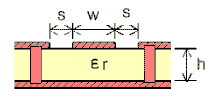
GUID-D026ACAE-C872-4BF7-BC8C-2CC223D4F5DF-low.gif Figure 10-4 Coplanar Waveguide (Cross Section)

Figure 10-5 shows the top view of the coplanar waveguide with GND and via stitching.

GUID-6F9EEE09-9A88-40C7-B0AF-D735652AEF5B-low.gif Figure 10-5 CPW With GND and Via Stitching (Top View)

The recommended values for the PCB are provided for 2-layer boards in Table 10-4 and 4-layer boards in Table 10-5.

Table 10-4 Recommended PCB Values for 2-Layer Board (L1 to L2 = 42.1 mils)
PARAMETER VALUE UNIT
W 24.5 mils
S 6.5 mils
H 42.1 mils
Er (FR-4 substrate) 4.8
Table 10-5 Recommended PCB Values for 4-Layer Board (L1 to L2 = 16 mils)
PARAMETER VALUE UNITS
W 21 mils
S 10 mils
H 16 mils
Er (FR-4 substrate) 4.5