ZHCSOK7B March 2020 – May 2021 CC3130
PRODUCTION DATA
- 1 特性
- 2 应用
- 3 说明
- 4 功能方框图
- 5 Revision History
- 6 Device Comparison
- 7 Terminal Configuration and Functions
-
8 Specifications
- 8.1 Absolute Maximum Ratings
- 8.2 ESD Ratings
- 8.3 Power-On Hours (POH)
- 8.4 Recommended Operating Conditions
- 8.5 Current Consumption Summary
- 8.6 TX Power Control
- 8.7 Brownout and Blackout Conditions
- 8.8 Electrical Characteristics for DIO Pins
- 8.9 Electrical Characteristics for Pin Internal Pullup and Pulldown
- 8.10 WLAN Receiver Characteristics
- 8.11 WLAN Transmitter Characteristics
- 8.12 WLAN Transmitter Out-of-Band Emissions
- 8.13 BLE/2.4 GHz Radio Coexistence and WLAN Coexistence Requirements
- 8.14 Thermal Resistance Characteristics for RGK Package
- 8.15
Timing and Switching Characteristics
- 8.15.1 Power Supply Sequencing
- 8.15.2 Device Reset
- 8.15.3 Reset Timing
- 8.15.4 Wakeup From HIBERNATE Mode
- 8.15.5 Clock Specifications
- 8.15.6 Interfaces
- 8.16 External Interfaces
- 9 Detailed Description
- 10Applications, Implementation, and Layout
- 11Device and Documentation Support
- 12Mechanical, Packaging, and Orderable Information
10.1.3 Typical Application
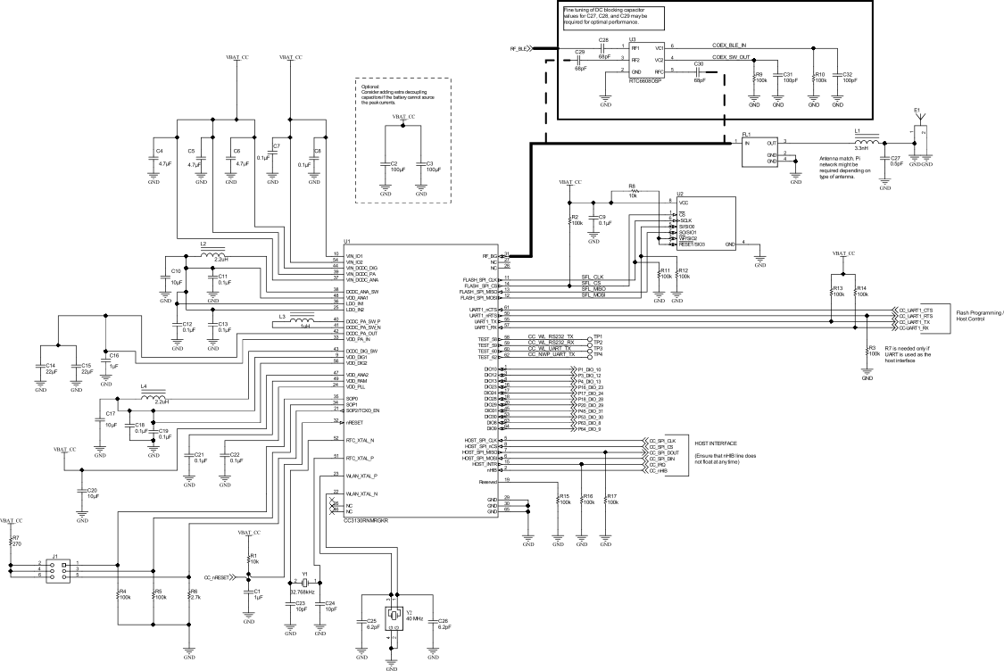
Figure 10-5 shows the schematic of the engine area for the CC3130 device in the wide-voltage mode of operation, and the optional RF implementations with BLE/2.4GHz coexistence. The corresponding Bill-of-Materials show in Table 10-1. For a full operation reference design, see the CC3235x SimpleLink™ and Internet of Things Hardware Design Files.
Note:
The Following guidelines are recommended for implementation of the RF design:
- Ensure an RF path is designed with an impedance of 50 Ω
- Tuning of the antenna impedance π matching network is recommended after manufacturing of the PCB to account for PCB parasitics
- π or L matching and tuning may be required between cascaded passive components on the RF path
 Figure 10-5 CC3130 Engine Area and Optional BLE Coexistence
Table 10-1 Bill-of-Materials for CC3130 Engine Area and Optional Coexistence
| QUANTITY | DESIGNATOR | VALUE | MANUFACTURER | PART NUMBER | DESCRIPTION |
|---|---|---|---|---|---|
| 1 | C1 | 1 µF | MuRata | GRM155R61A105KE15D | Capacitor, Ceramic, 1 µF, 10 V, ±10%, X5R, 0402 |
| 2 | C2, C3 | 100 µF | Taiyo Yuden | LMK325ABJ107MMHT | Capacitor, Ceramic, 100 µF, 10 V, ±20%, X5R, 1210 |
| 3 | C4, C5, C6 | 4.7 µF | TDK | C1005X5R0J475M050BC | Capacitor, Ceramic, 4.7 µF, 6.3 V, ±20%, X5R, 0402 |
| 10 | C7, C8, C9, C11, C12, C13, C18, C19, C21, C22 | 0.1 µF | TDK | C1005X5R1A104K050BA | Capacitor, Ceramic, 0.1 µF, 10 V, ±10%, X5R, 0402 |
| 3 | C10, C17, C20 | 10 µF | MuRata | GRM188R60J106ME47D | Capacitor, Ceramic, 10 µF, 6.3 V, ±20%, X5R, 0603 |
| 2 | C14, C15 | 22 µF | TDK | C1608X5R0G226M080AA | Capacitor, Ceramic, 22 µF, 4 V, ±20%, X5R, 0603 |
| 1 | C16 | 1 µF | TDK | C1005X5R1A105K050BB | Capacitor, Ceramic, 1 µF, 10 V, ±10%, X5R, 0402 |
| 2 | C23, C24 | 10 pF | MuRata | GRM1555C1H100JA01D | Capacitor, Ceramic, 10 pF, 50 V, ±5%, C0G/NP0, 0402 |
| 2 | C25, C26 | 6.2 pF | MuRata | GRM1555C1H6R2CA01D | Capacitor, Ceramic, 6.2 pF, 50 V, ±5%, C0G/NP0, 0402 |
| 1 | C27 | 0.5 pF | MuRata | GRM1555C1HR50BA01D | Capacitor, Ceramic, 0.5 pF, 50 V, ±20%, C0G/NP0, 0402 |
| 3 | C28(1), C29(1), C30(1) | 68 pF | MuRata | GRM0335C1H680JA1D | CAP, CERM, 68 pF, 50 V, +/- 5%, C0G/NP0, 0201 |
| 2 | C31(1), C32(1) | 100 pF | Yageo | CC0201JRNPO8BN101 | CAP, CERM, 100 pF, 25 V, +/- 5%, C0G/NP0, 0201 |
| 1 | E1 | 2.45-GHz Antenna | Taiyo Yuden | AH316M245001-T | ANT Bluetooth W-LAN Zigbee®, SMD |
| 1 | FL1 | 1.02 dB | TDK | DEA202450BT-1294C1-H | Multilayer Chip Band Pass Filter For 2.4 GHz W-LAN/Bluetooth, SMD |
| 1 | L1 | 3.3 nH | MuRata | LQG15HS3N3S02D | Inductor, Multilayer, Air Core, 3.3 nH, 0.3 A, 0.17 ohm, SMD |
| 2 | L2, L4 | 2.2 µH | MuRata | LQM2HPN2R2MG0L | Inductor, Multilayer, Ferrite, 2.2 µH, 1.3 A, 0.08 ohm, SMD |
| 1 | L3 | 1 µH | MuRata | LQM2HPN1R0MG0L | Inductor, Multilayer, Ferrite, 1 µH, 1.6 A, 0.055 ohm, SMD |
| 1 | R1, R8 | 10 k | Vishay-Dale | CRCW040210K0JNED | Resistor, 10 k, 5%, 0.063 W, 0402 |
| 13 | R2, R3, R4, R5, R9(1), R10(1), R11, R12, R13, R14, R15, R16, R17 | 100 k | Vishay-Dale | CRCW0402100KJNED | Resistor, 100 k, 5%, 0.063 W, 0402 |
| 1 | R6 | 2.7 k | Vishay-Dale | CRCW04022K70JNED | Resistor, 2.7 k, 5%, 0.063 W, 0402 |
| 1 | R7 | 270 | Vishay-Dale | CRCW0402270RJNED | Resistor, 270, 5%, 0.063 W, 0402 |
| 1 | U1 | MX25R | Macronix International Co., LTD | MX25R3235FM1IL0 | Ultra-Low Power, 32-Mbit [x 1/x 2/x 4] CMOS MXSMIO (Serial Multi I/O) Flash Memory, SOP-8 |
| 1 | U2 | CC3130 | Texas Instruments | CC3130RNMRGKR | SimpleLink™ Wi-Fi® Wireless Ntework Processor, RGK0064B |
| 1 | U3(1) | SPDT Switch | Richwave | RTC6608OSP | 0.03 GHz-6 GHz SPDT Switch |
| 1 | Y1 | Crystal | Abracon Corportation | ABS07-32.768KHZ-9-T | Crystal, 32.768 KHz, 9PF, SMD |
| 1 | Y2 | Crystal | Epson | Q24FA20H0039600 | Crystal, 40 MHz, 8pF, SMD |
(1) If the BLE/2.4 GHz Coexistence features is not used, these components are not required.