ZHCSJU5B February   2019  – May 2021 CC3135

PRODUCTION DATA  

  1. 特性
  2. 应用
  3. 说明
  4. 功能方框图
  5. Revision History
  6. Device Comparison
    1. 6.1 Related Products
  7. Terminal Configuration and Functions
    1. 7.1 Pin Diagram
    2. 7.2 Pin Attributes
    3. 7.3 Signal Descriptions
      1.      12
    4. 7.4 Connections for Unused Pins
  8. Specifications
    1. 8.1  Absolute Maximum Ratings
    2. 8.2  ESD Ratings
    3. 8.3  Power-On Hours (POH)
    4. 8.4  Recommended Operating Conditions
    5. 8.5  Current Consumption Summary: 2.4 GHz RF Band
    6. 8.6  Current Consumption Summary: 5 GHz RF Band
    7. 8.7  TX Power Control for 2.4 GHz Band
    8. 8.8  TX Power Control for 5 GHz
    9. 8.9  Brownout and Blackout Conditions
      1.      24
    10. 8.10 Electrical Characteristics for DIO Pins
      1.      26
      2.      27
    11. 8.11 Electrical Characteristics for Pin Internal Pullup and Pulldown
    12. 8.12 WLAN Receiver Characteristics
      1.      30
      2.      31
    13. 8.13 WLAN Transmitter Characteristics
      1.      33
      2.      34
    14. 8.14 WLAN Transmitter Out-of-Band Emissions
      1.      36
      2.      37
    15. 8.15 BLE/2.4 GHz Radio Coexistence and WLAN Coexistence Requirements
    16. 8.16 Thermal Resistance Characteristics for RGK Package
    17. 8.17 Timing and Switching Characteristics
      1. 8.17.1 Power Supply Sequencing
      2. 8.17.2 Device Reset
      3. 8.17.3 Reset Timing
        1. 8.17.3.1 nRESET (32-kHz Crystal)
        2.       45
        3. 8.17.3.2 nRESET (External 32-kHz Crystal)
          1.        47
      4. 8.17.4 Wakeup From HIBERNATE Mode
        1.       49
      5. 8.17.5 Clock Specifications
        1. 8.17.5.1 Slow Clock Using Internal Oscillator
          1.        52
        2. 8.17.5.2 Slow Clock Using an External Clock
          1.        54
        3. 8.17.5.3 Fast Clock (Fref) Using an External Crystal
          1.        56
        4. 8.17.5.4 Fast Clock (Fref) Using an External Oscillator
          1.        58
      6. 8.17.6 Interfaces
        1. 8.17.6.1 Host SPI Interface Timing
          1.        61
        2. 8.17.6.2 Flash SPI Interface Timing
          1.        63
        3. 8.17.6.3 DIO Interface Timing
          1. 8.17.6.3.1 DIO Output Transition Time Parameters (Vsupply = 3.3 V)
            1.         66
          2. 8.17.6.3.2 DIO Input Transition Time Parameters
            1.         68
    18. 8.18 External Interfaces
      1. 8.18.1 SPI Flash Interface
      2. 8.18.2 SPI Host Interface
      3. 8.18.3 Host UART Interface
        1. 8.18.3.1 5-Wire UART Topology
        2. 8.18.3.2 4-Wire UART Topology
        3. 8.18.3.3 3-Wire UART Topology
  9. Detailed Description
    1. 9.1 Overview
    2. 9.2 Device Features
      1. 9.2.1 WLAN
      2. 9.2.2 Network Stack
      3. 9.2.3 Security
      4. 9.2.4 Host Interface and Driver
      5. 9.2.5 System
    3. 9.3 FIPS 140-2 Level 1 Certification
    4. 9.4 Power-Management Subsystem
      1. 9.4.1 VBAT Wide-Voltage Connection
    5. 9.5 Low-Power Operating Modes
      1. 9.5.1 Low-Power Deep Sleep
      2. 9.5.2 Hibernate
      3. 9.5.3 Shutdown
    6. 9.6 Memory
      1. 9.6.1 External Memory Requirements
    7. 9.7 Restoring Factory Default Configuration
    8. 9.8 Hostless Mode
  10. 10Applications, Implementation, and Layout
    1. 10.1 Application Information
      1. 10.1.1 BLE/2.4 GHz Radio Coexistence
      2. 10.1.2 Antenna Selection
      3. 10.1.3 Typical Application
    2. 10.2 PCB Layout Guidelines
      1. 10.2.1 General PCB Guidelines
      2. 10.2.2 Power Layout and Routing
        1. 10.2.2.1 Design Considerations
      3. 10.2.3 Clock Interface Guidelines
      4. 10.2.4 Digital Input and Output Guidelines
      5. 10.2.5 RF Interface Guidelines
  11. 11Device and Documentation Support
    1. 11.1  第三方米6体育平台手机版_好二三四免责声明
    2. 11.2  Tools and Software
    3. 11.3  Firmware Updates
    4. 11.4  Device Nomenclature
    5. 11.5  Documentation Support
    6. 11.6  支持资源
    7. 11.7  Trademarks
    8. 11.8  静电放电警告
    9. 11.9  Export Control Notice
    10. 11.10 术语表
  12. 12Mechanical, Packaging, and Orderable Information
    1. 12.1 Packaging Information
    2. 12.2 Package Option Addendum
      1. 12.2.1 Packaging Information
      2. 12.2.2 Tape and Reel Information

封装选项

机械数据 (封装 | 引脚)
散热焊盘机械数据 (封装 | 引脚)
订购信息

SPI Host Interface

The device interfaces to an external host using the SPI interface. The CC3135 device can interrupt the host using the HOST_INTR line to initiate the data transfer over the interface. The SPI host interface can work up to a speed of 20 MHz.

Figure 8-17 shows the SPI host interface.
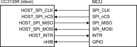
GUID-92F6A279-96EA-4EA0-BB56-A7DFEB2FF93F-low.gifFigure 8-17 SPI Host Interface


Table 8-23 lists the SPI host interface pins.

Table 8-23 SPI Host Interface
PIN NAMEDESCRIPTION
HOST_SPI_CLKClock (up to 20 MHz) from MCU host to CC3135 device
HOST_SPI_nCSCS (active low) signal from MCU host to CC3135 device
HOST_SPI_MOSIData from MCU host to CC3135 device
HOST_INTRInterrupt from CC3135 device to MCU host
HOST_SPI_MISOData from CC3135 device to MCU host
nHIBActive-low signal that commands the CC3135 device to enter hibernate mode (lowest power state)