ZHCSJU5B February   2019  – May 2021 CC3135

PRODUCTION DATA  

  1. 特性
  2. 应用
  3. 说明
  4. 功能方框图
  5. Revision History
  6. Device Comparison
    1. 6.1 Related Products
  7. Terminal Configuration and Functions
    1. 7.1 Pin Diagram
    2. 7.2 Pin Attributes
    3. 7.3 Signal Descriptions
      1.      12
    4. 7.4 Connections for Unused Pins
  8. Specifications
    1. 8.1  Absolute Maximum Ratings
    2. 8.2  ESD Ratings
    3. 8.3  Power-On Hours (POH)
    4. 8.4  Recommended Operating Conditions
    5. 8.5  Current Consumption Summary: 2.4 GHz RF Band
    6. 8.6  Current Consumption Summary: 5 GHz RF Band
    7. 8.7  TX Power Control for 2.4 GHz Band
    8. 8.8  TX Power Control for 5 GHz
    9. 8.9  Brownout and Blackout Conditions
      1.      24
    10. 8.10 Electrical Characteristics for DIO Pins
      1.      26
      2.      27
    11. 8.11 Electrical Characteristics for Pin Internal Pullup and Pulldown
    12. 8.12 WLAN Receiver Characteristics
      1.      30
      2.      31
    13. 8.13 WLAN Transmitter Characteristics
      1.      33
      2.      34
    14. 8.14 WLAN Transmitter Out-of-Band Emissions
      1.      36
      2.      37
    15. 8.15 BLE/2.4 GHz Radio Coexistence and WLAN Coexistence Requirements
    16. 8.16 Thermal Resistance Characteristics for RGK Package
    17. 8.17 Timing and Switching Characteristics
      1. 8.17.1 Power Supply Sequencing
      2. 8.17.2 Device Reset
      3. 8.17.3 Reset Timing
        1. 8.17.3.1 nRESET (32-kHz Crystal)
        2.       45
        3. 8.17.3.2 nRESET (External 32-kHz Crystal)
          1.        47
      4. 8.17.4 Wakeup From HIBERNATE Mode
        1.       49
      5. 8.17.5 Clock Specifications
        1. 8.17.5.1 Slow Clock Using Internal Oscillator
          1.        52
        2. 8.17.5.2 Slow Clock Using an External Clock
          1.        54
        3. 8.17.5.3 Fast Clock (Fref) Using an External Crystal
          1.        56
        4. 8.17.5.4 Fast Clock (Fref) Using an External Oscillator
          1.        58
      6. 8.17.6 Interfaces
        1. 8.17.6.1 Host SPI Interface Timing
          1.        61
        2. 8.17.6.2 Flash SPI Interface Timing
          1.        63
        3. 8.17.6.3 DIO Interface Timing
          1. 8.17.6.3.1 DIO Output Transition Time Parameters (Vsupply = 3.3 V)
            1.         66
          2. 8.17.6.3.2 DIO Input Transition Time Parameters
            1.         68
    18. 8.18 External Interfaces
      1. 8.18.1 SPI Flash Interface
      2. 8.18.2 SPI Host Interface
      3. 8.18.3 Host UART Interface
        1. 8.18.3.1 5-Wire UART Topology
        2. 8.18.3.2 4-Wire UART Topology
        3. 8.18.3.3 3-Wire UART Topology
  9. Detailed Description
    1. 9.1 Overview
    2. 9.2 Device Features
      1. 9.2.1 WLAN
      2. 9.2.2 Network Stack
      3. 9.2.3 Security
      4. 9.2.4 Host Interface and Driver
      5. 9.2.5 System
    3. 9.3 FIPS 140-2 Level 1 Certification
    4. 9.4 Power-Management Subsystem
      1. 9.4.1 VBAT Wide-Voltage Connection
    5. 9.5 Low-Power Operating Modes
      1. 9.5.1 Low-Power Deep Sleep
      2. 9.5.2 Hibernate
      3. 9.5.3 Shutdown
    6. 9.6 Memory
      1. 9.6.1 External Memory Requirements
    7. 9.7 Restoring Factory Default Configuration
    8. 9.8 Hostless Mode
  10. 10Applications, Implementation, and Layout
    1. 10.1 Application Information
      1. 10.1.1 BLE/2.4 GHz Radio Coexistence
      2. 10.1.2 Antenna Selection
      3. 10.1.3 Typical Application
    2. 10.2 PCB Layout Guidelines
      1. 10.2.1 General PCB Guidelines
      2. 10.2.2 Power Layout and Routing
        1. 10.2.2.1 Design Considerations
      3. 10.2.3 Clock Interface Guidelines
      4. 10.2.4 Digital Input and Output Guidelines
      5. 10.2.5 RF Interface Guidelines
  11. 11Device and Documentation Support
    1. 11.1  第三方米6体育平台手机版_好二三四免责声明
    2. 11.2  Tools and Software
    3. 11.3  Firmware Updates
    4. 11.4  Device Nomenclature
    5. 11.5  Documentation Support
    6. 11.6  支持资源
    7. 11.7  Trademarks
    8. 11.8  静电放电警告
    9. 11.9  Export Control Notice
    10. 11.10 术语表
  12. 12Mechanical, Packaging, and Orderable Information
    1. 12.1 Packaging Information
    2. 12.2 Package Option Addendum
      1. 12.2.1 Packaging Information
      2. 12.2.2 Tape and Reel Information

封装选项

机械数据 (封装 | 引脚)
散热焊盘机械数据 (封装 | 引脚)
订购信息

Brownout and Blackout Conditions

The device enters a brownout condition when the input voltage drops below Vbrownout (see Figure 8-4 and Figure 8-5). This condition must be considered during design of the power supply routing, especially when operating from a battery. High-current operations, such as a TX packet or any external activity (not necessarily related directly to networking) can cause a drop in the supply voltage, potentially triggering a brownout condition. The resistance includes the internal resistance of the battery, the contact resistance of the battery holder (four contacts for 2× AA batteries), and the wiring and PCB routing resistance.

Note:

When the device is in HIBERNATE state, brownout is not detected. Only blackout is in effect during HIBERNATE state.
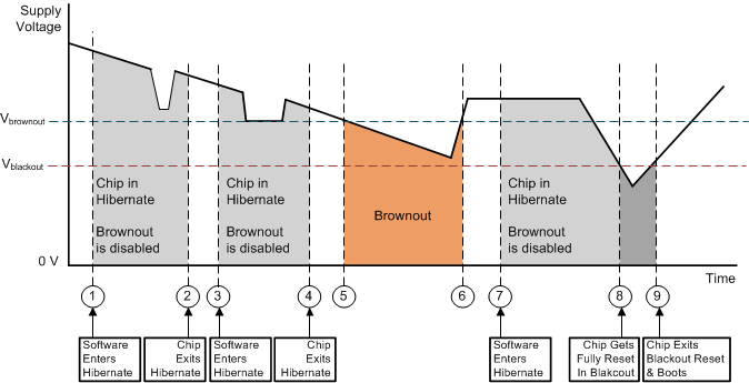
GUID-740E3145-E3B2-40ED-80B7-7681249CB98C-low.gifFigure 8-4 Brownout and Blackout Levels (1 of 2)
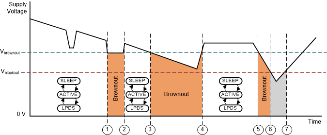


GUID-B7323AF0-50BC-4C9A-B4FF-D69EA68040BB-low.gifFigure 8-5 Brownout and Blackout Levels (2 of 2)

In the brownout condition, all sections of the device (including the 32-kHz RTC) shut down except for the Hibernate module, which remains on. The current in this state can reach approximately 400 µA. The blackout condition is equivalent to a hardware reset event in which all states within the device are lost.

Table 8-1 lists the brownout and blackout voltage levels.