ZHCSJU5B February   2019  – May 2021 CC3135

PRODUCTION DATA  

  1. 特性
  2. 应用
  3. 说明
  4. 功能方框图
  5. Revision History
  6. Device Comparison
    1. 6.1 Related Products
  7. Terminal Configuration and Functions
    1. 7.1 Pin Diagram
    2. 7.2 Pin Attributes
    3. 7.3 Signal Descriptions
      1.      12
    4. 7.4 Connections for Unused Pins
  8. Specifications
    1. 8.1  Absolute Maximum Ratings
    2. 8.2  ESD Ratings
    3. 8.3  Power-On Hours (POH)
    4. 8.4  Recommended Operating Conditions
    5. 8.5  Current Consumption Summary: 2.4 GHz RF Band
    6. 8.6  Current Consumption Summary: 5 GHz RF Band
    7. 8.7  TX Power Control for 2.4 GHz Band
    8. 8.8  TX Power Control for 5 GHz
    9. 8.9  Brownout and Blackout Conditions
      1.      24
    10. 8.10 Electrical Characteristics for DIO Pins
      1.      26
      2.      27
    11. 8.11 Electrical Characteristics for Pin Internal Pullup and Pulldown
    12. 8.12 WLAN Receiver Characteristics
      1.      30
      2.      31
    13. 8.13 WLAN Transmitter Characteristics
      1.      33
      2.      34
    14. 8.14 WLAN Transmitter Out-of-Band Emissions
      1.      36
      2.      37
    15. 8.15 BLE/2.4 GHz Radio Coexistence and WLAN Coexistence Requirements
    16. 8.16 Thermal Resistance Characteristics for RGK Package
    17. 8.17 Timing and Switching Characteristics
      1. 8.17.1 Power Supply Sequencing
      2. 8.17.2 Device Reset
      3. 8.17.3 Reset Timing
        1. 8.17.3.1 nRESET (32-kHz Crystal)
        2.       45
        3. 8.17.3.2 nRESET (External 32-kHz Crystal)
          1.        47
      4. 8.17.4 Wakeup From HIBERNATE Mode
        1.       49
      5. 8.17.5 Clock Specifications
        1. 8.17.5.1 Slow Clock Using Internal Oscillator
          1.        52
        2. 8.17.5.2 Slow Clock Using an External Clock
          1.        54
        3. 8.17.5.3 Fast Clock (Fref) Using an External Crystal
          1.        56
        4. 8.17.5.4 Fast Clock (Fref) Using an External Oscillator
          1.        58
      6. 8.17.6 Interfaces
        1. 8.17.6.1 Host SPI Interface Timing
          1.        61
        2. 8.17.6.2 Flash SPI Interface Timing
          1.        63
        3. 8.17.6.3 DIO Interface Timing
          1. 8.17.6.3.1 DIO Output Transition Time Parameters (Vsupply = 3.3 V)
            1.         66
          2. 8.17.6.3.2 DIO Input Transition Time Parameters
            1.         68
    18. 8.18 External Interfaces
      1. 8.18.1 SPI Flash Interface
      2. 8.18.2 SPI Host Interface
      3. 8.18.3 Host UART Interface
        1. 8.18.3.1 5-Wire UART Topology
        2. 8.18.3.2 4-Wire UART Topology
        3. 8.18.3.3 3-Wire UART Topology
  9. Detailed Description
    1. 9.1 Overview
    2. 9.2 Device Features
      1. 9.2.1 WLAN
      2. 9.2.2 Network Stack
      3. 9.2.3 Security
      4. 9.2.4 Host Interface and Driver
      5. 9.2.5 System
    3. 9.3 FIPS 140-2 Level 1 Certification
    4. 9.4 Power-Management Subsystem
      1. 9.4.1 VBAT Wide-Voltage Connection
    5. 9.5 Low-Power Operating Modes
      1. 9.5.1 Low-Power Deep Sleep
      2. 9.5.2 Hibernate
      3. 9.5.3 Shutdown
    6. 9.6 Memory
      1. 9.6.1 External Memory Requirements
    7. 9.7 Restoring Factory Default Configuration
    8. 9.8 Hostless Mode
  10. 10Applications, Implementation, and Layout
    1. 10.1 Application Information
      1. 10.1.1 BLE/2.4 GHz Radio Coexistence
      2. 10.1.2 Antenna Selection
      3. 10.1.3 Typical Application
    2. 10.2 PCB Layout Guidelines
      1. 10.2.1 General PCB Guidelines
      2. 10.2.2 Power Layout and Routing
        1. 10.2.2.1 Design Considerations
      3. 10.2.3 Clock Interface Guidelines
      4. 10.2.4 Digital Input and Output Guidelines
      5. 10.2.5 RF Interface Guidelines
  11. 11Device and Documentation Support
    1. 11.1  第三方米6体育平台手机版_好二三四免责声明
    2. 11.2  Tools and Software
    3. 11.3  Firmware Updates
    4. 11.4  Device Nomenclature
    5. 11.5  Documentation Support
    6. 11.6  支持资源
    7. 11.7  Trademarks
    8. 11.8  静电放电警告
    9. 11.9  Export Control Notice
    10. 11.10 术语表
  12. 12Mechanical, Packaging, and Orderable Information
    1. 12.1 Packaging Information
    2. 12.2 Package Option Addendum
      1. 12.2.1 Packaging Information
      2. 12.2.2 Tape and Reel Information

封装选项

机械数据 (封装 | 引脚)
散热焊盘机械数据 (封装 | 引脚)
订购信息

Antenna Selection

The CC3135 device is designed to also support antenna selection and is controlled from Image Creator. When enabled, there are 3 options possible options:

  • ANT 1: When selected, the GPIOs that are defined for antenna selection with set the RF path for antenna 1.
  • ANT 2: When selected, the GPIOs that are defined for antenna selection will set the RF path for antenna 2.
  • Autoselect: When selected, during a scan and prior to connecting to an AP, CC3135 device will determine the best RF path and select the appropriate antenna (12)(13). The result is the saved as port of the profile.

Figure 10-5 shows the implementation of a complete Bluetooth® low energy and WLAN coexistence network with the WLAN operating on either a 2.4- or a 5 GHz band with antenna selection. The SOP lines control the 5 GHz switch. The Coex switch is controlled by a GPIO signal from the BLE device and a GPIO signal from the CC3135 device. The Antenna switch is controlled by 2 GPIO lines from the CC3135 device.
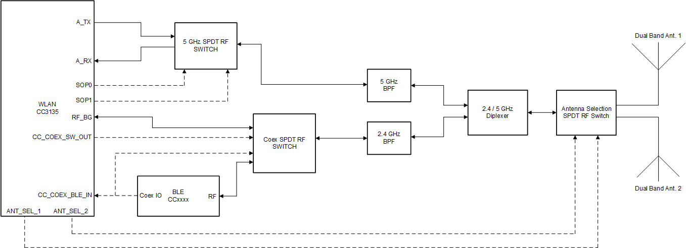
GUID-41779B5F-C376-41C1-973C-F335B96F0B2D-low.gifFigure 10-5 Antenna Selection Solution with Coexistence Solution and 5 GHz Wi-Fi®


Figure 10-6 shows the antenna selection implementation for Wi-Fi®, with BLE operating on it's own antenna. The SOP lines control the 5 GHz switch. Note in this implementation no Coex switch is required and only a single GPIO from the BLE device to the CC3135 device is required. The Antenna switch is controlled by 2 GPIO lines from the CC3135 device.
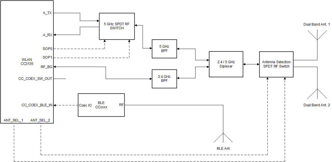
GUID-0C013AFC-0161-483C-BCDD-3F4705F6C3E7-low.gifFigure 10-6 Coexistence Solution with Wi-Fi Antenna Selection and Dedicated BLE Antenna
When selecting Autoselect via the API, a reset is required in order for the CC3135 device to determine the best antenna for use.