ZHCSM61C November   2014  – September 2020 CC3200MOD

PRODUCTION DATA  

  1. 特性
  2. 应用
  3. 说明
  4. Functional Block Diagrams
  5. Revision History
  6. Device Comparison
    1. 6.1 Related Products
  7. Terminal Configuration and Functions
    1. 7.1 CC3200MOD Pin Diagram
    2. 7.2 Pin Attributes
      1. 7.2.1 Module Pin Attributes
    3. 7.3 Pin Attributes and Pin Multiplexing
    4. 7.4 Recommended Pin Multiplexing Configurations
      1. 7.4.1 ADC Reference Accuracy Specifications
    5. 7.5 Drive Strength and Reset States for Analog-Digital Multiplexed Pins
    6. 7.6 Pad State After Application of Power to Chip, but Before Reset Release
  8. Specifications
    1. 8.1  Absolute Maximum Ratings
    2. 8.2  ESD Ratings
    3. 8.3  Power-On Hours (POH)
    4. 8.4  Recommended Operating Conditions
    5. 8.5  Power Consumption Summary
      1. 8.5.1 Current Consumption
    6. 8.6  Brownout and Blackout Conditions
    7. 8.7  WLAN RF Characteristics
      1. 8.7.1 WLAN Receiver Characteristics
      2. 8.7.2 WLAN Transmitter Characteristics
    8. 8.8  Reset Requirement
    9. 8.9  Thermal Resistance Characteristics for MOB and MON Packages
    10. 8.10 Timing and Switching Characteristics
      1. 8.10.1 nRESET
      2. 8.10.2 Wake Up From Hibernate Timing
  9. Detailed Description
    1. 9.1 Overview
    2. 9.2 Functional Block Diagram
    3. 9.3 Arm® Cortex®-M4 处理器内核子系统
    4. 9.4 CC3200 Device Encryption
    5. 9.5 Wi-Fi® Network Processor Subsystem
    6. 9.6 Power-Management Subsystem
      1. 9.6.1 VBAT Wide-Voltage Connection
    7. 9.7 Low-Power Operating Mode
    8. 9.8 Memory
      1. 9.8.1 External Memory Requirements
      2. 9.8.2 Internal Memory
        1. 9.8.2.1 SRAM
        2. 9.8.2.2 ROM
        3. 9.8.2.3 Memory Map
    9. 9.9 Boot Modes
      1. 9.9.1 Overview
      2. 9.9.2 Invocation Sequence and Boot Mode Selection
      3. 9.9.3 Boot Mode List
  10. 10Applications, Implementation, and Layout
    1. 10.1 Device Connection and Layout Fundamentals
      1. 10.1.1 Power Supply Decoupling and Bulk Capacitors
      2. 10.1.2 Reset
      3. 10.1.3 Unused Pins
      4. 10.1.4 General Layout Recommendations
      5. 10.1.5 Do's and Don'ts
    2. 10.2 Reference Schematics
    3. 10.3 Design Requirements
    4. 10.4 Detailed Design Procedure
    5. 10.5 Layout Recommendations
      1. 10.5.1 RF Section (Placement and Routing)
      2. 10.5.2 Antenna Placement and Routing
      3. 10.5.3 Transmission Line
  11. 11Environmental Requirements and Specifications
    1. 11.1 PCB Bending
    2. 11.2 Handling Environment
      1. 11.2.1 Terminals
      2. 11.2.2 Falling
    3. 11.3 Storage Condition
      1. 11.3.1 Moisture Barrier Bag Before Opened
      2. 11.3.2 Moisture Barrier Bag Open
    4. 11.4 Baking Conditions
    5. 11.5 Soldering and Reflow Condition
  12. 12Device and Documentation Support
    1. 12.1 Device Support
      1. 12.1.1 Development Support
      2. 12.1.2 Firmware Updates
    2. 12.2 Device Nomenclature
    3. 12.3 Documentation Support
    4. 12.4 Trademarks
  13. 13Mechanical, Packaging, and Orderable Information
    1. 13.1 Mechanical Drawing
    2. 13.2 Package Option
      1. 13.2.1 Packaging Information
      2. 13.2.2 Tape and Reel Information

请参考 PDF 数据表获取器件具体的封装图。

机械数据 (封装 | 引脚)
  • MOB|63
散热焊盘机械数据 (封装 | 引脚)

Wake Up From Hibernate Timing

Table 8-3 lists the software hibernate timing requirements.

Note:

The 32.768-kHz crystal is kept enabled by default when the module goes to hibernate.

Table 8-3 Software Hibernate Timing Requirements
ITEM NAME DESCRIPTION MIN TYP MAX UNIT
THIB_MIN Minimum hibernate time The time for which the device must be held in hibernate mode 10 ms
T2 Hardware wake-up time Time taken by the hardware to initialize 25 ms
T3 Firmware initiation time Time taken by the ROM firmware to initialize the hardware 3 ms
T4 Code download time Time taken to download the code from the serial flash to on-chip RAM Image size (KB) × 0.75 ms


Figure 8-7 shows the timing diagram for wake up from the hibernate state.
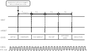
GUID-E5256EAF-1C35-41A6-8312-7C64B28B8148-low.gif Figure 8-7 Wake Up From Hibernate Timing Diagram