ZHCSJ35C September   2016  – May 2021 CC3220R , CC3220S , CC3220SF

PRODUCTION DATA  

  1. 特性
  2. 应用
  3. 说明
  4. 功能方框图
  5. Revision History
  6. Device Comparison
    1. 6.1 Related Products
  7. Terminal Configuration and Functions
    1. 7.1 Pin Diagram
    2. 7.2 Pin Attributes and Pin Multiplexing
      1. 7.2.1 Pin Descriptions
    3. 7.3 Signal Descriptions
      1. 7.3.1 Signal Descriptions
    4. 7.4 Pin Multiplexing
    5. 7.5 Drive Strength and Reset States for Analog and Digital Multiplexed Pins
    6. 7.6 Pad State After Application of Power to Chip But Before Reset Release
    7. 7.7 Connections for Unused Pins
  8. Specifications
    1. 8.1  Absolute Maximum Ratings
    2. 8.2  ESD Ratings
    3. 8.3  Power-On Hours (POH)
    4. 8.4  Recommended Operating Conditions
    5. 8.5  Current Consumption Summary (CC3220R, CC3220S)
    6. 8.6  Current Consumption Summary (CC3220SF)
    7. 8.7  TX Power and IBAT versus TX Power Level Settings
    8. 8.8  Brownout and Blackout Conditions
    9. 8.9  Electrical Characteristics (3.3 V, 25°C)
    10. 8.10 WLAN Receiver Characteristics
    11. 8.11 WLAN Transmitter Characteristics
    12. 8.12 WLAN Filter Requirements
      1. 8.12.1 WLAN Filter Requirements
    13. 8.13 Thermal Resistance Characteristics
      1. 8.13.1 Thermal Resistance Characteristics for RGK Package
    14. 8.14 Timing and Switching Characteristics
      1. 8.14.1 Power Supply Sequencing
      2. 8.14.2 Device Reset
      3. 8.14.3 Reset Timing
        1. 8.14.3.1 nRESET (32-kHz Crystal)
        2. 8.14.3.2 First-Time Power-Up and Reset Removal Timing Requirements (32-kHz Crystal)
        3. 8.14.3.3 nRESET (External 32-kHz)
          1. 8.14.3.3.1 First-Time Power-Up and Reset Removal Timing Requirements (External 32-kHz)
      4. 8.14.4 Wakeup From HIBERNATE Mode
      5. 8.14.5 Clock Specifications
        1. 8.14.5.1 Slow Clock Using Internal Oscillator
          1. 8.14.5.1.1 RTC Crystal Requirements
        2. 8.14.5.2 Slow Clock Using an External Clock
          1. 8.14.5.2.1 External RTC Digital Clock Requirements
        3. 8.14.5.3 Fast Clock (Fref) Using an External Crystal
          1. 8.14.5.3.1 WLAN Fast-Clock Crystal Requirements
        4. 8.14.5.4 Fast Clock (Fref) Using an External Oscillator
          1. 8.14.5.4.1 External Fref Clock Requirements (–40°C to +85°C)
      6. 8.14.6 Peripherals Timing
        1. 8.14.6.1  SPI
          1. 8.14.6.1.1 SPI Master
            1. 8.14.6.1.1.1 SPI Master Timing Parameters
          2. 8.14.6.1.2 SPI Slave
            1. 8.14.6.1.2.1 SPI Slave Timing Parameters
        2. 8.14.6.2  I2S
          1. 8.14.6.2.1 I2S Transmit Mode
            1. 8.14.6.2.1.1 I2S Transmit Mode Timing Parameters
          2. 8.14.6.2.2 I2S Receive Mode
            1. 8.14.6.2.2.1 I2S Receive Mode Timing Parameters
        3. 8.14.6.3  GPIOs
          1. 8.14.6.3.1 GPIO Output Transition Time Parameters (Vsupply = 3.3 V)
            1. 8.14.6.3.1.1 GPIO Output Transition Times (Vsupply = 3.3 V) (1) (1)
          2. 8.14.6.3.2 GPIO Output Transition Time Parameters (Vsupply = 1.85 V)
            1. 8.14.6.3.2.1 GPIO Output Transition Times (Vsupply = 1.85 V) (1) (1)
          3. 8.14.6.3.3 GPIO Input Transition Time Parameters
            1. 8.14.6.3.3.1 GPIO Input Transition Time Parameters'
        4. 8.14.6.4  I2C
          1. 8.14.6.4.1 I2C Timing Parameters (1)
        5. 8.14.6.5  IEEE 1149.1 JTAG
          1. 8.14.6.5.1 JTAG Timing Parameters
        6. 8.14.6.6  ADC
          1. 8.14.6.6.1 ADC Electrical Specifications
        7. 8.14.6.7  Camera Parallel Port
          1. 8.14.6.7.1 Camera Parallel Port Timing Parameters
        8. 8.14.6.8  UART
        9. 8.14.6.9  SD Host
        10. 8.14.6.10 Timers
  9. Detailed Description
    1. 9.1 Arm® Cortex®-M4 Processor Core Subsystem
    2. 9.2 Wi-Fi Network Processor Subsystem
      1. 9.2.1 WLAN
      2. 9.2.2 Network Stack
    3. 9.3 Security
    4. 9.4 Power-Management Subsystem
      1. 9.4.1 VBAT Wide-Voltage Connection
      2. 9.4.2 Preregulated 1.85-V Connection
    5. 9.5 Low-Power Operating Mode
    6. 9.6 Memory
      1. 9.6.1 External Memory Requirements
      2. 9.6.2 Internal Memory
        1. 9.6.2.1 SRAM
        2. 9.6.2.2 ROM
        3. 9.6.2.3 Flash Memory
        4. 9.6.2.4 Memory Map
    7. 9.7 Restoring Factory Default Configuration
    8. 9.8 Boot Modes
      1. 9.8.1 Boot Mode List
  10. 10Applications, Implementation, and Layout
    1. 10.1 Application Information
      1. 10.1.1 Typical Application —CC3220x Wide-Voltage Mode
      2. 10.1.2 Typical Application Schematic—CC3220x Preregulated, 1.85-V Mode
    2. 10.2 PCB Layout Guidelines
      1. 10.2.1 General PCB Guidelines
      2. 10.2.2 Power Layout and Routing
        1. 10.2.2.1 Design Considerations
      3. 10.2.3 Clock Interfaces
      4. 10.2.4 Digital Input and Output
      5. 10.2.5 RF Interface
  11. 11Device and Documentation Support
    1. 11.1 Development Tools and Software
    2. 11.2 Firmware Updates
    3. 11.3 Device Nomenclature
    4. 11.4 Documentation Support
    5. 11.5 支持资源
    6. 11.6 Trademarks
    7. 11.7 Electrostatic Discharge Caution
    8. 11.8 Export Control Notice
    9. 11.9 术语表
  12. 12Mechanical, Packaging, and Orderable Information
    1. 12.1 Packaging Information

封装选项

机械数据 (封装 | 引脚)
散热焊盘机械数据 (封装 | 引脚)
订购信息

Design Considerations

The following design guidelines must be followed when laying out the CC3220x device:

  • Route all of the input decoupling capacitors (C11, C13, and C18) on L2 using thick traces, to isolate the RF ground from the noisy supply ground. This step is also required to meet the IEEE spectral mask specifications.
  • Maintain the thickness of power traces to be greater than 12 mils. Take special consideration for power amplifier supply lines (pins 33, 40, 41, and 42), and all input supply pins (pins 37, 39, and 44).
  • Ensure the shortest grounding loop for the PLL supply decoupling capacitor (pin 24).
  • Place all decoupling capacitors as close to the respective pins as possible.
  • Power budget: The CC3220x device can consume up to 450 mA for 3.3 V, 670 mA for 2.1 V, and 700 mA for 1.85 V, for 24 ms during the calibration cycle.
  • Ensure the power supply is designed to source this current without any issues. The complete calibration (TX and RX) can take up to 17 mJ of energy from the battery over a time of 24 ms.
  • The CC3220x device contains many high-current input pins. Ensure the trace feeding these pins is capable of handling the following currents:
    • VIN_DCDC_PA input (pin 39) maximum is 1 A
    • VIN_DCDC_ANA input (pin 37) maximum is 600 mA
    • VIN_DCDC_DIG input (pin 44) maximum is 500 mA
    • DCDC_PA_SW_P (pin 40) and DCDC_PA_SW_N (pin 41) switching nodes maximum is 1 A
    • DCDC_PA_OUT output node (pin 42) maximum 1 A
    • DCDC_ANA_SW switching node (pin 38) maximum is 600 mA
    • DCDC_DIG_SW switching node (pin 43) maximum is 500 mA
    • VDD_PA_IN supply (pin 33) maximum is 500 mA

Figure 10-3 shows the ground routing for the input decoupling capacitors.
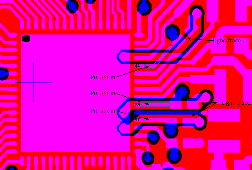
GUID-BB3B0A06-A6A3-4C93-BD4A-BB00B7629013-low.pngFigure 10-3 Ground Routing for the Input Decoupling Capacitors

The ground return for the input capacitors are routed on L2 to reduce the EMI and improve the spectral mask. This routing must be strictly followed because it is critical for the overall performance of the device.