ZHCS994B June 2012 – September 2018 CC430F5123 , CC430F5125 , CC430F5143 , CC430F5145 , CC430F5147 , CC430F6147
PRODUCTION DATA.
- 1器件概述
- 2修订历史记录
- 3Device Comparison
- 4Terminal Configuration and Functions
-
5Specifications
- 5.1 Absolute Maximum Ratings
- 5.2 ESD Ratings
- 5.3 Recommended Operating Conditions
- 5.4 Active Mode Supply Current Into VCC Excluding External Current
- 5.5 Typical Characteristics – Active Mode Supply Currents
- 5.6 Low-Power Mode Supply Currents (Into VCC) Excluding External Current
- 5.7 Typical Characteristics – Low-Power Mode Supply Currents
- 5.8 Low-Power Mode With LCD Supply Currents (Into VCC) Excluding External Current
- 5.9 Thermal Resistance Characteristics, CC430F51xx
- 5.10 Thermal Resistance Characteristics, CC430F61xx
- 5.11 Digital Inputs
- 5.12 Digital Outputs
- 5.13 Typical Characteristics – Outputs, Reduced Drive Strength (PxDS.y = 0)
- 5.14 Typical Characteristics – Outputs, Full Drive Strength (PxDS.y = 1)
- 5.15 Crystal Oscillator, XT1, Low-Frequency Mode
- 5.16 Internal Very-Low-Power Low-Frequency Oscillator (VLO)
- 5.17 Internal Reference, Low-Frequency Oscillator (REFO)
- 5.18 DCO Frequency
- 5.19 PMM, Brownout Reset (BOR)
- 5.20 PMM, Core Voltage
- 5.21 PMM, SVS High Side
- 5.22 PMM, SVM High Side
- 5.23 PMM, SVS Low Side
- 5.24 PMM, SVM Low Side
- 5.25 Wake-up Times From Low-Power Modes and Reset
- 5.26 Timer_A
- 5.27 USCI (UART Mode) Clock Frequency
- 5.28 USCI (UART Mode)
- 5.29 USCI (SPI Master Mode) Clock Frequency
- 5.30 USCI (SPI Master Mode)
- 5.31 USCI (SPI Slave Mode)
- 5.32 USCI (I2C Mode)
- 5.33 LCD_B Operating Conditions
- 5.34 LCD_B Electrical Characteristics
- 5.35 10-Bit ADC, Power Supply and Input Range Conditions
- 5.36 10-Bit ADC, Timing Parameters
- 5.37 10-Bit ADC, Linearity Parameters
- 5.38 REF, External Reference
- 5.39 REF, Built-In Reference
- 5.40 Comparator_B
- 5.41 Flash Memory
- 5.42 JTAG and Spy-Bi-Wire Interface
- 5.43
RF1A CC1101-Based Radio Parameters
- 5.43.1 RF1A Recommended Operating Conditions
- 5.43.2 RF Crystal Oscillator, XT2
- 5.43.3 Current Consumption, Reduced-Power Modes
- 5.43.4 Current Consumption, Receive Mode
- 5.43.5 Current Consumption, Transmit Mode
- 5.43.6 Typical TX Current Consumption, 315 MHz, 25°C
- 5.43.7 Typical TX Current Consumption, 433 MHz, 25°C
- 5.43.8 Typical TX Current Consumption, 868 MHz
- 5.43.9 Typical TX Current Consumption, 915 MHz
- 5.43.10 RF Receive, Overall
- 5.43.11 RF Receive, 315 MHz
- 5.43.12 RF Receive, 433 MHz
- 5.43.13 RF Receive, 868 MHz and 915 MHz
- 5.43.14 Typical Sensitivity, 315 MHz, Sensitivity Optimized Setting
- 5.43.15 Typical Sensitivity, 433 MHz, Sensitivity Optimized Setting
- 5.43.16 Typical Sensitivity, 868 MHz, Sensitivity Optimized Setting
- 5.43.17 Typical Sensitivity, 915 MHz, Sensitivity Optimized Setting
- 5.43.18 RF Transmit
- 5.43.19 Optimum PATABLE Settings for Various Output Power Levels and Frequency Bands
- 5.43.20 Typical Output Power, 315 MHz
- 5.43.21 Typical Output Power, 433 MHz
- 5.43.22 Typical Output Power, 868 MHz
- 5.43.23 Typical Output Power, 915 MHz
- 5.43.24 Frequency Synthesizer Characteristics
- 5.43.25 Typical RSSI_offset Values
-
6Detailed Description
- 6.1 Sub-1 GHz Radio
- 6.2 CPU
- 6.3 Operating Modes
- 6.4 Interrupt Vector Addresses
- 6.5 Memory Organization
- 6.6 Bootloader (BSL)
- 6.7 JTAG Operation
- 6.8 Flash Memory
- 6.9 RAM
- 6.10 Backup RAM
- 6.11
Peripherals
- 6.11.1 Oscillator and System Clock
- 6.11.2 Power-Management Module (PMM)
- 6.11.3 Digital I/O
- 6.11.4 Port Mapping Controller
- 6.11.5 System Module (SYS)
- 6.11.6 DMA Controller
- 6.11.7 Watchdog Timer (WDT_A)
- 6.11.8 CRC16
- 6.11.9 Hardware Multiplier
- 6.11.10 AES128 Accelerator
- 6.11.11 Universal Serial Communication Interface (USCI)
- 6.11.12 TA0
- 6.11.13 TA1
- 6.11.14 Real-Time Clock (RTC_D)
- 6.11.15 Voltage Reference (REF) (Including Output)
- 6.11.16 LCD_B (Only CC430F614x)
- 6.11.17 Comparator_B
- 6.11.18 ADC10_A (CC430F614x and CC430F514x Only)
- 6.11.19 Embedded Emulation Module (EEM) (S Version)
- 6.11.20 Peripheral File Map
- 6.12
Input/Output Diagrams
- 6.12.1 Port P1 (P1.0 to P1.4) Input/Output With Schmitt Trigger
- 6.12.2 Port P1 (P1.5 to P1.7) Input/Output With Schmitt Trigger
- 6.12.3 Port P2 (P2.0 to P2.7) Input/Output With Schmitt Trigger
- 6.12.4 Port P3 (P3.0 to P3.7) Input/Output With Schmitt Trigger
- 6.12.5 Port P4 (P4.0 to P4.7) Input/Output With Schmitt Trigger (CC430F614x Only)
- 6.12.6 Port P5 (P5.0 and P5.1) Input/Output With Schmitt Trigger
- 6.12.7 Port P5 (P5.2 to P5.4) Input/Output With Schmitt Trigger (CC430F614x Only)
- 6.12.8 Port P5 (P5.5 to P5.7) Input/Output With Schmitt Trigger (CC430F614x Only)
- 6.12.9 Port PJ (PJ.0) JTAG Pin TDO, Input/Output With Schmitt Trigger or Output
- 6.12.10 Port PJ (PJ.1 to PJ.3) JTAG Pins TMS, TCK, TDI/TCLK, Input/Output With Schmitt Trigger or Output
- 6.13 Device Descriptor Structure
- 7Applications, Implementation, and Layout
- 8器件和文档支持
- 9机械,封装和可订购信息
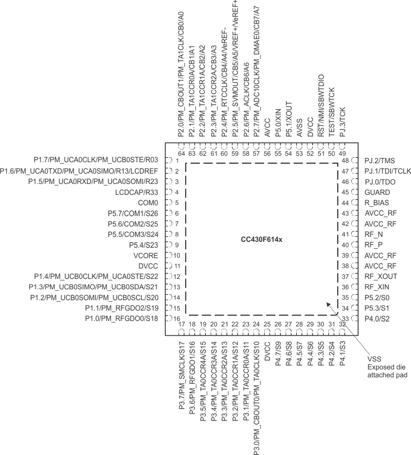
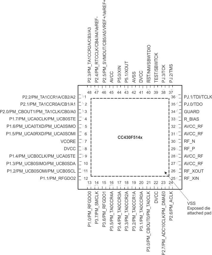
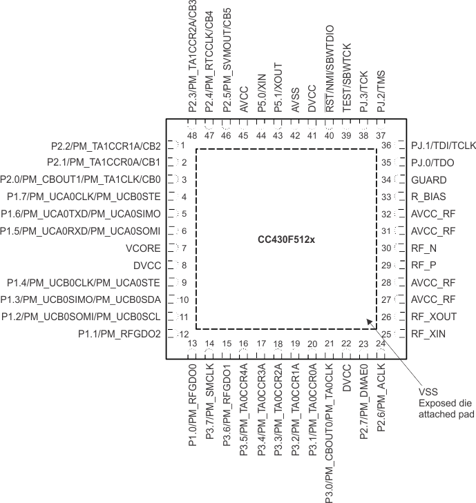
4.1 Pin Diagrams
Figure 4-1 shows the pinout for the CC430F614x devices in the RGC package.

CAUTION:
LCDCAP/R33 must be connected to VSS if not used.NOTE:
The secondary digital functions on ports P1, P2, and P3 are fully mappable. Pinout shows only the default mapping. See Table 6-6 for details.Figure 4-2 shows the pinout for the CC430F514x devices in the RGZ package.

NOTE:
The secondary digital functions on ports P1, P2, and P3 are fully mappable. Pinout shows only the default mapping. See Table 6-6 for details.Figure 4-3 shows the pinout for the CC430F512x devices in the RGZ package.

NOTE:
The secondary digital functions on ports P1, P2, and P3 are fully mappable. Pinout shows only the default mapping. See Table 6-6 for details.